Crosstalk is an unavoidable phenomenon in high-speed digital circuits and densely routed PCBs. In practical design work, it is often discussed as a set of rules—such as increasing trace spacing, routing orthogonally, or placing ground traces nearby—while the physical reasons why these rules work are rarely explained in depth.
As a result, crosstalk tends to be treated as “noise handled by experience.”
Before discussing countermeasures, this article organizes the root causes of crosstalk at the circuit level. The key point is that crosstalk is not a special or accidental phenomenon, but rather an inevitable consequence of parasitic elements that do not appear in schematic diagrams.
Definition of Crosstalk
Crosstalk is a phenomenon in which the time-varying behavior of one signal trace induces unwanted voltage or current in an adjacent trace.
What is important here is that the signal traces are not connected in a DC sense, and that data is not physically “leaking” from one trace to another. Crosstalk occurs due to electromagnetic coupling. Therefore, as long as traces exist on a PCB, crosstalk can never be reduced to zero.
Superficial Explanations vs. the Underlying Mechanism
Crosstalk is often explained in the following ways:
- “It occurs because traces are close together.”
- “It is unavoidable with high-speed signals.”
- “It is an EMC problem.”
While these statements are not incorrect as descriptions of the phenomenon, they do not explain the cause-and-effect relationships required for design decisions. If one cannot explain why closer spacing worsens crosstalk, why rise time matters, or why termination and ground structures change the result, design rules become nothing more than a checklist.
The Essence of Crosstalk: Coupling via Parasitic Elements
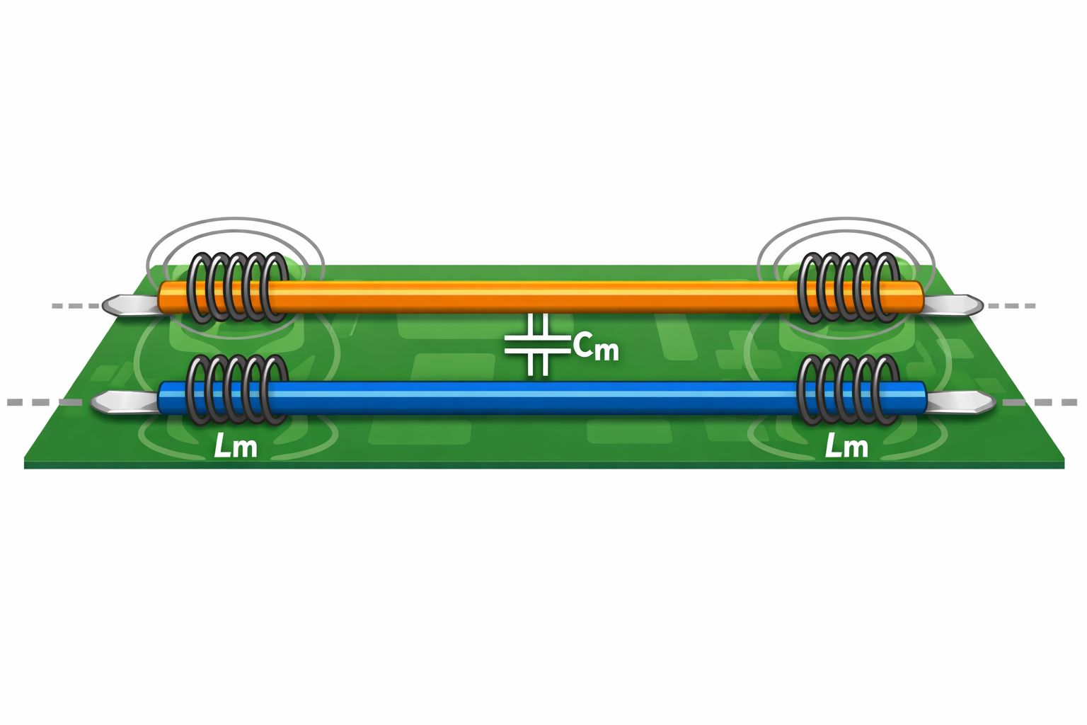
The cause of crosstalk is clear. Unintended parasitic elements are formed between signal traces. On a real PCB, coupling capacitance (Cm) appears between adjacent traces, and coupling inductance (Lm) is formed between current loops that include the signal trace and its return path.
In schematic diagrams, each signal trace is represented as an independent net. In actual hardware, however, traces share physical space and operate while generating electric and magnetic fields. As a result, voltage changes affect adjacent traces through electric fields, and current changes affect other trace loops through magnetic fields.
Crosstalk is a phenomenon in which signal energy is coupled through these parasitic elements that do not appear in schematics. The following figure schematically illustrates coupling that “does not exist in the schematic, but inevitably exists in real hardware.”
Electric-Field Coupling and Magnetic-Field Coupling
Coupling through parasitic elements can be divided into two mechanisms with different characteristics.
Electric-Field Coupling (Capacitive Coupling)
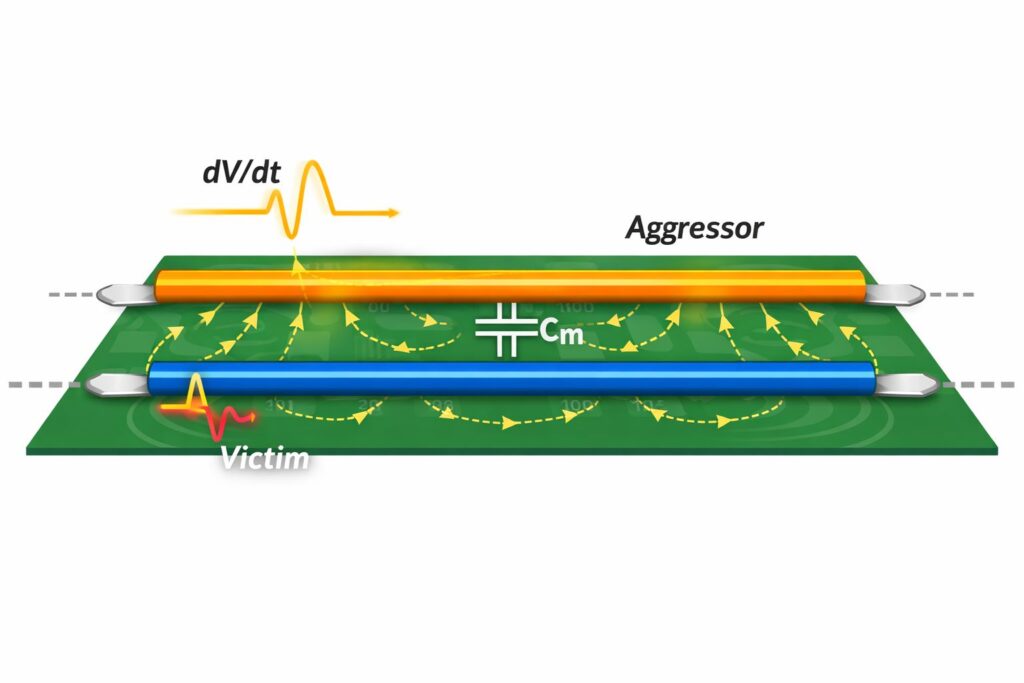
Electric-field coupling occurs through coupling capacitance Cm formed between adjacent traces. When the voltage on a signal trace changes with time, an electric field spreads around the trace and influences neighboring traces.
The important point is that the magnitude of the effect depends not on the absolute voltage level, but on the rate of voltage change (dV/dt). The steeper the rising or falling edge, the larger the voltage induced on the adjacent trace through the coupling capacitance.
In the figure below, the electric field expands in response to the voltage transition on the aggressor trace, and part of it couples into the victim trace. The noise observed on the victim trace typically occurs at the same timing as the aggressor’s signal edge.
Magnetic-Field Coupling (Inductive Coupling)
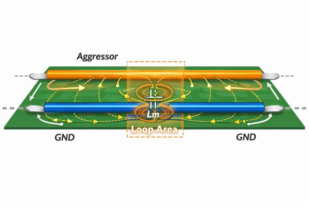
Magnetic-field coupling occurs when current loops formed by signal traces and their return paths (GND) are coupled via magnetic flux. When current changes with time, a magnetic field is generated around the loop, which can influence neighboring loops.
The dominant factor in magnetic-field coupling is the loop area. As the distance between the signal trace and the ground return increases, the loop area becomes larger, and the coupling inductance Lm increases accordingly.
The figure below shows how different ground routing strategies change the loop shape and the amount of magnetic coupling. Design rules such as placing the ground close to the signal and ensuring a continuous return path reduce magnetic coupling by minimizing the loop area.
Why Rise Time Becomes the Dominant Factor
Crosstalk depends very little on the absolute signal level. What dominates is the time-derivative component.
- Electric-field coupling: time variation of voltage (dV/dt)
- Magnetic-field coupling: time variation of current (dI/dt)
Therefore, even at low clock frequencies, crosstalk becomes significant if the signal edges are fast. This is why the explanation “high-speed signals cause problems because of high frequency” is incomplete.
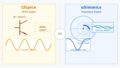
What Can Be Visualized with uSimmics
uSimmics (formerly QucsStudio) is not a tool for accurately predicting the absolute amount of crosstalk on a real PCB. However, it allows us to observe—separately in the time domain— the waveforms produced by coupling capacitance only, coupling inductance only, and the combination of both.
This is extremely effective for understanding what causes crosstalk and which element is dominant. What matters is not numerical accuracy, but the ability to clearly identify which parasitic element is active and at what timing.
Summary
In this article, crosstalk was organized not as the result of design rules, but as a cause-and-effect relationship at the circuit level.
Crosstalk is not a special noise phenomenon; it is an inevitable electromagnetic coupling that occurs whenever traces exist.
On real PCBs, coupling capacitance (Cm) is formed between adjacent traces, and coupling inductance (Lm) exists between current loops formed by signal traces and their return paths. Even though these parasitic elements do not appear in schematics, they are always present.
Electric-field coupling mainly depends on voltage variation (dV/dt), while magnetic-field coupling depends on current variation (dI/dt) and loop area. As a result, the magnitude of crosstalk is governed more strongly by rise time and return-path structure than by the signal frequency itself.
Design measures such as increasing trace spacing, placing ground traces closer, and adding termination resistors are not merely empirical rules. They can be understood as physical methods for reducing coupling through parasitic elements.
Now the full flow is connected: cause → waveform → countermeasure. If you want to review the overall picture, it’s best to go back to the first article and read through again.
▶ Back: Noise Countermeasures Basics: What Are Decoupling Caps, Ferrite Beads, and GND Planes For?

Comment