
The Create Matching Circuit feature in uSimmics (formerly QucsStudio) automatically designs a matching network for circuits with impedance mismatch. This guide uses a 50 Ω to 25 Ω matching example to walk through circuit generation, S-parameter simulation, and interactive parameter tuning.
What You’ll Learn
- The basic concept of impedance matching and why it matters in RF circuits
- How to launch and configure the Create Matching Circuit feature
- How to place the auto-generated LC matching circuit into a schematic
- How to verify matching performance with S-parameter simulation
- How to fine-tune component values using the Parameter Tuning window
What Is Impedance Matching?
Impedance matching is the practice of making the impedances of a signal source, transmission line, and load equal to each other. This maximizes power transfer and minimizes reflections. In RF and microwave circuits, impedance mismatch causes signal reflections that degrade performance and can damage transmitter stages in some cases.
Matching networks are typically implemented as LC circuits that transform impedance at a specified frequency.
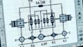
Step 1: Creating a Test Circuit
First, create a circuit with intentional impedance mismatch.
- Launch uSimmics (formerly QucsStudio).
- From Components → Lumped Components, drag a resistor onto the schematic.
- Double-click the resistor and change its value to 25 Ω (from the default 50 Ω).
- From Sources, place a Power Source. Leave its output impedance at the default 50 Ω.
- Connect GND to each component.
- Wire the components together to complete the circuit.
This creates a circuit with a 50 Ω source and a 25 Ω load — a mismatched condition where some signal power is reflected.
Step 2: Designing the Matching Circuit
2-1. Opening the Create Matching Circuit Window
- In the menu bar, click Tools.
- Select Matching Circuit → Create Matching Circuit.
- The Create Matching Circuit window opens.
2-2. Setting Matching Conditions
Configure the following parameters:
| Parameter | Value | Description |
|---|---|---|
| Impedance 1 | 50 Ω | Source-side impedance (Port 1). |
| Impedance 2 | 25 Ω | Load-side impedance (Port 2). Matches the 25 Ω load used in the test circuit. |
| Frequency | 1 GHz | Target frequency for the matching network. |
2-3. Generating the Matching Circuit
Click Create. uSimmics (formerly QucsStudio) automatically computes an LC matching network and copies it to the clipboard.
Step 3: Placing and Connecting the Matching Circuit
- Press Ctrl + V on the schematic containing the 25 Ω load to paste the matching circuit.
- Connect the output of the matching circuit to the 25 Ω load.
- Connect the input of the matching circuit to the 50 Ω source.
Typical auto-generated values for 1 GHz, 50 Ω → 25 Ω matching:
- Series inductor: approximately 40 nH
- Shunt capacitor: approximately 32 pF
Step 4: Running the Simulation
4-1. Configuring the S-Parameter Simulation
- From Simulations, select S-parameter Simulation and place it on the schematic.
- Double-click the simulation component and set the following parameters:
| Setting | Value |
|---|---|
| Start frequency | 50 MHz |
| Stop frequency | 150 MHz |
| Frequency step | 1 MHz |
4-2. Executing the Simulation
Click the gear icon or select Simulate → Simulate from the menu to run the simulation.
Step 5: Reviewing Simulation Results
After simulation completes, S-parameter graphs and a Smith chart appear.
5-1. Adding Markers
- Right-click on the graph and select Set Marker on Graph.
- Click on the data curve to place a marker.
- Move the marker to 100 MHz (near the target matching frequency).
5-2. Key Metrics to Check
| Parameter | Target | Interpretation |
|---|---|---|
| S11 (return loss) | Below −20 dB | Low reflection at the input indicates good matching. −20 dB or better is considered excellent. |
| S21 (insertion loss) | Near 0 dB | Indicates efficient signal transmission through the matching network. |
Step 6: Optimizing with Parameter Tuning
You can interactively adjust the auto-generated component values to achieve more precise matching.
6-1. Opening the Tuning Window
- From the menu, select Simulation → Tune.
- Click on the inductor in the schematic, then click on the capacitor.
- The Parameter Tuning window opens.
6-2. Setting the Tuning Range
| Component | Minimum | Maximum |
|---|---|---|
| Inductor | 1 nH | 100 nH |
| Capacitor | 1 pF | 100 pF |
6-3. Performing the Tuning
- Move the sliders up and down to vary component values.
- Watch the Smith chart and S11 graph update in real time.
- Aim to minimize S11 (move the Smith chart trace toward the center) as you adjust.
- The optimum values near 40 nH and 32 pF confirm the auto-calculated results.
Design Notes
- The circuit generated by Create Matching Circuit is an ideal LC network. Real components have parasitic effects (coil parasitic capacitance, capacitor parasitic inductance, etc.) that are not modeled. For GHz-band designs, supplement with S-parameter-based simulation using real component data.
- Matching bandwidth depends on the Q-factor and order of the LC network. For wideband matching, consider a multi-stage matching network.
- The Smith chart is an essential RF design tool that represents complex impedance and reflection coefficient on a circular chart. The center represents perfect matching (S11 = 0).
Related Articles
- How to Use Filter Synthesis in uSimmics (formerly QucsStudio) [2026]
- How to Use Qucsattenuator in uSimmics (formerly QucsStudio) [2026]
- How to Use the Transmission Line Calculator in uSimmics (formerly QucsStudio) [2026]
- How to Import S-Parameter Files in uSimmics (formerly QucsStudio) [2026]
- How to Export S-Parameters in uSimmics (formerly QucsStudio) [2026]

Comment