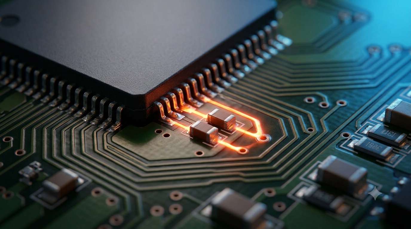
“Place the decoupling capacitor close to the IC.”
Every circuit-design textbook says this. Yet surprisingly few explain why it has to be close. If you only remember it as “a rule,” you won’t be able to adapt when you hit a problem during layout.
In this article we explain how a decoupling capacitor works and why it must be placed “close,” from the standpoint of parasitic inductance, and confirm it as waveforms with uSimmics simulations.
What Is a Decoupling Capacitor? — The IC’s “Instant Charger”
In one sentence, the role of a decoupling (bypass) capacitor is to be a “local power source” that quickly supplies current the moment the IC suddenly needs it.
When a digital IC switches, it draws a large current from the supply in an instant. If that current has to come from a distant power source, the inductance on the power and GND lines gets in the way and the voltage swings significantly (this is the ground bounce covered in the previous article).
If a decoupling capacitor sits right next to the IC, the IC can draw charge from “the capacitor in front of it” instead of “the distant supply.” Because a capacitor can release charge with almost zero inductance, the voltage swing is greatly suppressed.
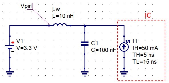
Between the capacitor and the IC there are board traces. These traces always have inductance. The farther the IC and the capacitor are apart, the larger this inductance becomes. From here on we denote this wiring-derived inductance as L_wire.
When a capacitor and an inductance are in series, they form an LC circuit. At high frequencies this inductance becomes a large impedance that impedes current flow into the capacitor. In other words, the “farther” the capacitor is from the IC, the less effective it becomes at high frequencies.
The Capacitor Itself Also Has Parasitic Inductance
Another point to watch is that the capacitor body itself has equivalent series inductance (ESL). From here on we denote this as L_esl. The ESL of a chip capacitor is around 0.5–1 nH, but a leaded capacitor reaches 5–20 nH or more.
Because of this ESL, a capacitor has an “upper frequency at which it can still behave as a capacitor” (its self-resonant frequency). Above that frequency, the capacitor behaves as an inductor.
The reason chip ceramic capacitors are recommended for decoupling is precisely that their ESL is small, so they keep working up to high frequencies.
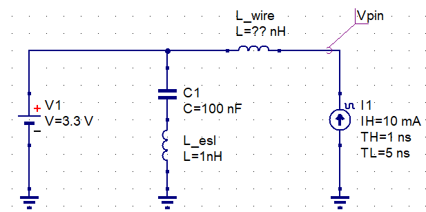
The two parasitic inductances introduced so far — the wiring-derived L_wire and the capacitor’s own L_esl — appear in series, as shown below. Combined with the capacitor’s C, the real equivalent circuit turns out to be an LC circuit with “C, L_wire, and L_esl” in series.
Verifying with uSimmics — How the Effect Changes with Distance
Experiment 1: Varying the Distance of the Decoupling Capacitor
Let’s see with a simulation how much it actually changes.
We build the following circuit in uSimmics:
- A voltage source (VCC = 3.3 V)
- A current source that emulates the IC’s switching (rise time 1 ns)
- An inductor that emulates the trace between the IC and the capacitor (L_wire)
- A decoupling capacitor (C = 0.1 μF, ESL = 1 nH)
- Observation node: the voltage at the IC’s power pin
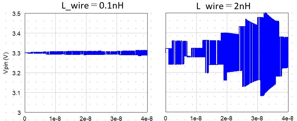
What the waveforms confirm:
- The closer the capacitor (small L_wire), the more the supply-voltage swing is suppressed.
- When the capacitor is far (large L_wire), there are cases where it has almost no effect even though it is present.
- The ringing period lengthens in proportion to the wiring inductance (the LC resonant frequency drops).
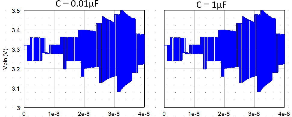
Experiment 2: Varying the Capacitance
Two-Stage Placement Is the Answer — Covering the Frequency Band
Since it is hard to cover the whole frequency band with a single decoupling capacitor, the basic approach is to place decoupling capacitors in two stages.
Stage 1: Board Entry Point (Low-Frequency Coverage)
Placed right after the power enters the board. Its purposes are:
- Filtering noise that has entered from external wiring
- Lowering the low-frequency component of the board’s overall power impedance
Parts used: aluminum electrolytic or tantalum capacitors of a few tens of μF. If needed, combine with an inductor to form an LC filter.
Stage 2: Right Next to the IC (High-Frequency Coverage)
Placed right beside the IC’s power and GND pins. Its purposes are:
- Instantly supplying the IC’s switching current
- Lowering the power impedance in the high-frequency region
Parts used: 0.01–0.1 μF chip ceramic capacitors (prioritize low ESL). As a rule, place one per IC. For ICs that draw little current and run slowly, one per two or three ICs is acceptable.
When You Make Stage 2 Two Capacitors
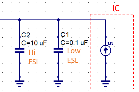
If you want the high-frequency coverage to span a wider band, you can use two types of capacitor at stage 2 (for example 0.1 μF + 0.001 μF). In that case, place the smaller-value capacitor on the side closer to the IC. A smaller capacitor has a higher self-resonant frequency and is therefore effective against very high frequencies.
Practical Layout Notes
How Close Is “Close”?
A rough guide is within 2–3 mm of the IC’s power and GND pins. Watch out for cases where the routing of board traces makes the effective distance longer.
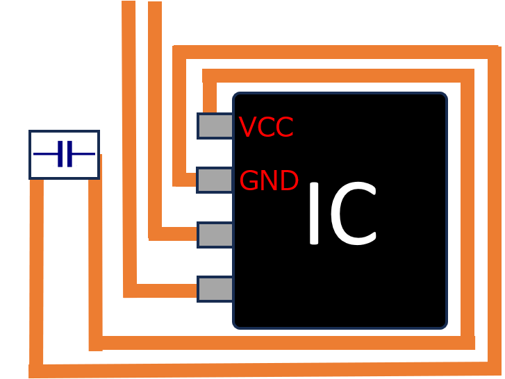
What matters here is not that the placement looks close, but that the trace path the current actually flows through is as short as possible. Even if you place the capacitor right next to the IC, if the traces to power and GND are routed the long way around, the distance as a current path becomes long and the parasitic inductance increases just the same. Conversely, even with some space in between, if the wiring is straight and short the effect is preserved. Your criterion should be “the length of the wiring path,” not “physical closeness.”
The GND Via Position Matters Too
On a multilayer board, place the via that connects the capacitor’s GND side to the ground plane as close to directly under the capacitor as possible. If the via is far away, the trace in between also becomes inductance.
Summary
- A decoupling capacitor is a “local power source” that instantly supplies the IC’s switching current and suppresses supply-voltage fluctuation.
- The farther it is from the IC, the more wiring inductance increases and the more its high-frequency effect is lost — that is why you “place it close.”
- The capacitor’s own ESL also limits the high-frequency behavior, so use chip ceramic capacitors.
- Two-stage placement (large capacitance at the board entry + small capacitance right next to the IC) covers a wide frequency band.
Not just “put in a decoupling capacitor,” but thinking through “where, what, and in how many stages” is what matters in real noise mitigation.

Comment