
“GND is supposed to be 0 V — so why does noise show up?”
When I first started designing circuits, I wondered the same thing. GND is the reference potential — a fixed 0 V point. Yet in real hardware the GND potential wobbles, and that becomes a source of noise. This phenomenon is called ground bounce.
In this article we look at why ground bounce happens, verifying the underlying principle with uSimmics (QucsStudio) simulations.
A Circuit Is a “Loop” — Current Flows in GND Too
Let’s start from the fundamentals.
An electronic circuit forms, as the name implies, a “circuit” — a loop. Current leaves the power supply, passes through ICs and components to make them work, and returns to the supply through ground.
In a schematic the GND symbol is drawn as “the reference point = 0 V,” and the return line is usually omitted. But that omitted line physically exists on the real board as copper foil and traces.

This fact is the starting point for understanding ground bounce.
GND Wiring Has “Impedance”
The impedance of an ideal conductor is zero. Real wires and PCB traces are not ideal.
Wiring always has inductance. The DC resistance is negligibly small even for a thin trace, but the impedance from inductance (Z = jωL) grows as the frequency rises. In modern circuits, where ICs switch at high speed, this inductance reaches values you cannot ignore.
Even a single straight trace has roughly 1 nH/mm of inductance. A 10 mm GND trace, for example, is about 10 nH — around 6.3 Ω of impedance at 100 MHz.

The True Nature of Ground Bounce — V = L × di/dt
When current flows through a trace that has inductance, a voltage appears whenever the current changes. As a formula:
V = L × di/dtHere L is the inductance and di/dt is the rate of change of current over time.
When a digital IC switches, the supply current changes abruptly. The instant an output flips Low → High, the IC draws current from the supply all at once. When that steep current change flows through the inductance of the GND trace, a voltage appears — exactly as the formula says.
The ground potential, which should be 0 V, momentarily jumps up or dips down. That is ground bounce.

The Same Problem Happens on the Power Rail
Despite the name “ground” bounce, the identical phenomenon occurs on the power line. If a changing current flows through the inductance of the power trace, the supply voltage fluctuates the same way. Power and ground are symmetrical, so both need the same countermeasures.
Verifying with uSimmics — GND Impedance and Bounce Waveforms
Let’s confirm the effect with an actual simulation.
Circuit Configuration
We build the following circuit in uSimmics:
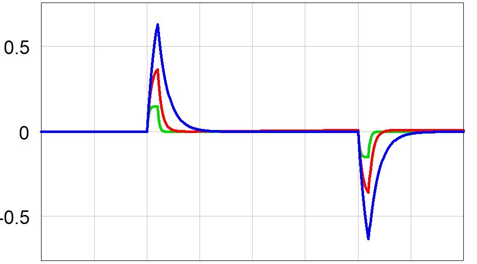
- A current source that emulates the IC’s switching (rise time 1 ns, peak current 50 mA)
- An inductor that emulates the GND trace (L = 10 nH)
- Observation node: the voltage on the GND trace

Simulation Results

What the waveform tells us:
- The larger the rate of current change (di/dt), the larger the GND fluctuation (bounce).
- The larger the inductance L (the longer the trace), the greater the bounce for the same current change.
- After the bounce, ringing appears — LC resonance between L and the stray capacitance C.
Comparing Different Values of L
Increasing L as 1 → 10 → 30 nH grows the amplitude as 0.05 → 0.43 → 0.73 V, showing that the inductance of the GND return path directly determines the amount of bounce.

Common Impedance — Bounce Affects Other Circuits Too
Ground bounce becomes even more serious when multiple circuits share the same GND.
When the switching current of circuit A flows through the shared GND trace (the common impedance), the resulting voltage fluctuation also shifts the ground potential of circuit B. From circuit B’s point of view its GND wobbles even though it did nothing itself — a cause of malfunction. This is called common-impedance coupling.

Countermeasures for Ground Bounce
Once the cause is clear, so is the direction of the fix. From V = L × di/dt, there are three effective approaches.
① Place a Decoupling Capacitor Close to the IC
Rather than supplying the IC’s switching current from a distant power source, supply it instantly from a capacitor placed right next to the IC. Because the capacitor stores charge, it can respond quickly to sudden current demands.
The key word is close. Place the decoupling cap far from the IC and the wiring inductance in between sharply reduces its effectiveness at high frequencies.
→ For the placement and effectiveness of decoupling capacitors, see the next article, Why Are Decoupling Capacitors Placed Close to the IC?
② Lower the Inductance of the GND Wiring
To lower inductance, the basics are to make the wiring short, wide, and straight.
On a PCB, turning the GND into a solid pattern (a ground plane) is the most effective. A planar solid pattern has far lower impedance than a linear trace and dramatically suppresses ground bounce. In a 4-layer board, dedicating one layer to a solid GND plane is standard practice.
③ Slow Down di/dt
Make the current change more gradual and the value of L × di/dt shrinks. You can reduce the IC’s output drive strength, or insert a ferrite bead to soften the signal edge. This trades off against signal speed, however, so for digital signals it calls for careful judgment.
Summary
The key points of ground bounce:
- GND is the “reference potential,” but real wiring has inductance.
- When switching current changes abruptly, the GND potential fluctuates through V = L × di/dt — this is ground bounce.
- When several circuits share a GND, interference spreads through the common impedance.
- Countermeasures: ① place decoupling caps close to the IC, ② lower the GND inductance (solid plane), ③ slow down di/dt.
Treat GND as “just a 0 V line” and noise problems will make your life hard. Designing GND as a “conductor that has impedance,” exactly like a signal line, is the first step toward noise-resilient boards.


Comment