- What Is “Reflection” in High-Speed Signals?
- The Root Cause of Reflection: Impedance Mismatch
- Viewing Only Reflection with a Minimal Circuit
- How to Build This in uSimmics
- Why Reflections Are Easier to See at the Source End
- Waveform Comparison: How the Step Changes with RL
- When Reflections Become a Problem
- Summary: Reflections Appear as Steps at the Source End
What Is “Reflection” in High-Speed Signals?
In high-speed digital signals, a trace does not behave as a simple wire but as a transmission line. As a result, depending on the termination condition, part of the signal energy can be sent back toward the source. This phenomenon is called reflection.
Reflection is not a case of “noise being mixed in.” It is a physically natural phenomenon in which signal energy changes direction due to impedance mismatch.
In this article, we reproduce reflection using a minimal circuit and understand it as a visible “step” in the waveform.
The Root Cause of Reflection: Impedance Mismatch
A transmission line has a characteristic impedance Z0. If the load resistance RL at the receiving end does not match Z0, part of the arriving signal is not absorbed and instead travels back toward the source.
This returning signal is the reflected wave. The magnitude and polarity of the reflection are determined by the relationship between Z0 and RL.
Viewing Only Reflection with a Minimal Circuit
To observe reflection as clearly as possible, the load is kept as a pure resistor. By avoiding capacitive elements such as input capacitance, we eliminate ringing caused by LC resonance.
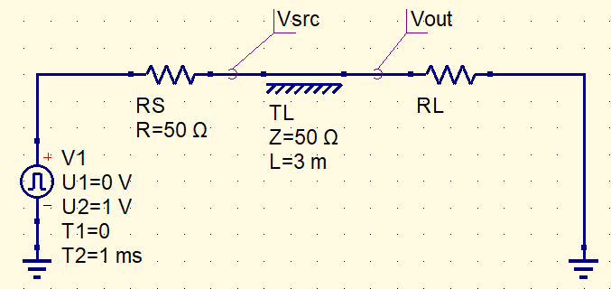
Minimal circuit for observing reflection
Vpulse ── Rs ──●── TL ── RL ── GND
               │
        Vsrc (main observation point)
In this article, the main observation point is the junction between Rs and the transmission line (TL), i.e., the source end. Since the reflected wave returns after a delay, it appears very clearly as a step change at this point.
How to Build This in uSimmics
1. Place the Components
- Pulse / VPulse (pulse voltage source)
- Resistor ×2 (Rs, RL)
- Transmission Line (Coaxial Line / RLCG Line, etc.)
- GND
- Voltage Probe (for Vsrc)
2. Transmission Line Delay
In uSimmics, many transmission line components do not require you to specify delay directly. Instead, the delay is automatically determined by the line length L and the relative permittivity er.
The propagation delay Td is given by:
Td = (L / c) × √er
For FR-4–like material (er ≈ 4), the delay is approximately 6.7 ns per meter. In this article, the line length is chosen so that the delay is about 10 ns, making reflections easier to observe.
3. Example Parameter Settings
- Vpulse: 0 → 1 V, Tr = 0.1 ns, Tf = 0.1 ns
- Rs: 50 Ω
- TL: Length L = 1.5 m (≈ 10 ns delay)
- RL: 50 Ω → 100 Ω → 1 kΩ → 25 Ω (comparison)
Why Reflections Are Easier to See at the Source End
Reflections are generated at the load end, but they are not always visible there as a clear “step.”
At the source end, the incident wave appears first. Then, after the round-trip delay, the reflected wave returns later. Because of this time difference, the voltage changes again after the initial transition, making the reflection clearly visible as a step.
At the load end, although reflection does occur, the reflected wave immediately travels back along the transmission line. Since it does not stay at that point, it may be difficult to observe as a step depending on conditions.
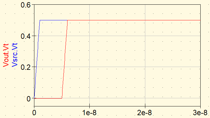
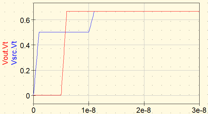
Waveform Comparison: How the Step Changes with RL
Observe Vout while changing only RL. Reflections appear as a delayed change in the waveform — a visible step.
Case 1: RL = 50 Ω (Matched)
Since RL matches Z0 (50 Ω), reflection is minimal. Vout rises cleanly without noticeable steps.
Case 2: RL = 100 Ω (Mismatch: Higher Load)
Reflection occurs, and a step appears after the initial rise. Compared to the matched case, the voltage increases slightly after a delay.
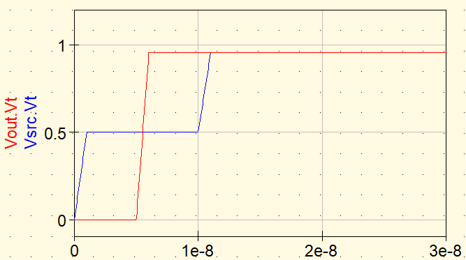
Case 3: RL = 1 kΩ (Nearly Open)
The closer the load is to open, the stronger the reflection becomes. The step in Vout is very clear. This is the easiest case for first experiencing reflection behavior.
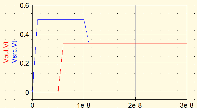
Case 4: RL = 25 Ω (Mismatch: Lower Load)
In this case, the step appears in the opposite direction. Reflections do not always “jump upward”; their polarity depends on the termination condition. Reflection is observed as a delayed step, and both its magnitude and direction are determined by the load impedance.
When Reflections Become a Problem
Reflections become problematic not because the frequency is high, but because the rise time is fast. As ICs become faster, reflections can no longer be ignored even on the same physical traces.
Situations like “it used to work before, but now it’s unstable” are often caused by shorter rise times.
Summary: Reflections Appear as Steps at the Source End
- Reflections are caused by impedance mismatch at the load end
- The source end (junction of Rs and TL) is where steps are easiest to observe
- Delay is determined by er and line length, and governs the return timing of reflections
- Starting with a minimal, resistor-only circuit is the fastest way to understand reflections
Rather than focusing only on where reflections occur,
pay attention to where they are observed.
This perspective makes it much easier to correctly interpret waveform behavior.
Once reflection makes sense, the next topic is ringing. We’ll reproduce only the oscillation component that becomes confusing when it’s mixed with reflection.
▶ Next: What Is Ringing? Reproduce the Oscillation with uSimmics and Understand It


Comment