
Static electricity is noise everyone has experienced. Yet few people can say why it destroys semiconductors, or what the discharge current actually looks like.
This article covers the basics of electrostatic discharge (ESD) and surge, explains the discharge current waveform from the equivalent circuit of the machine model (MM), and goes on to how protection devices are chosen. In the MM the inductance of the discharge path matters and produces a damped oscillation, which makes it a good vehicle for understanding, from the circuit, why the waveform rings.
- Where static electricity comes from
- There is more than one discharge model — HBM and MM
- The machine model — a metal discharge as an equivalent circuit
- The discharge waveform — damped oscillation and damping
- Why it destroys semiconductors
- Choosing ESD and surge protection devices
- Placing protection devices, and how to think about it
- ESD control in manufacturing
- Summary
- Related Articles
Where static electricity comes from
Static electricity is generated by friction between insulators (triboelectric charging). Plastic floors, carpets, synthetic-fibre clothing — the insulators around us charge readily. It is not only the human body: metal objects also charge, including production equipment, jigs and tools.
What governs how much charge builds up is humidity. Dry air is an excellent insulator; when humidity is high, the air itself becomes less insulating and accumulated charge leaks away on its own. That is why static is so common in the dry winter months.
When a charged object touches a terminal of a piece of equipment, the stored charge discharges all at once. That energy is more than enough to destroy a semiconductor device.
There is more than one discharge model — HBM and MM
The equivalent circuit for an electrostatic discharge depends on what is discharging. Two models are standard.
- Human body model (HBM): a discharge from the fingertip of a charged person. The standard (ANSI/ESDA/JEDEC JS-001) specifies C = 100 pF and R = 1.5 kΩ. Because the resistance is large, the waveform is a non-oscillatory exponential decay.
- Machine model (MM): a discharge from a charged metal object such as equipment or a jig. C = 200 pF, R ≈ 0 Ω. Metal-to-metal discharge leaves almost no resistance, so the discharge path inductance resonates and the waveform becomes a damped oscillation.
In this article we work through the MM, where the effect of inductance — the damped oscillation — shows up clearly in the equivalent circuit.
The machine model — a metal discharge as an equivalent circuit
The machine model represents a charged metal object as a C–R–L circuit. The charge stored on the metal (C) discharges all at once through the resistance (R) and the inductance (L) of the discharge path.
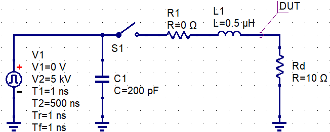
What each element means (machine model, MM):
- C (equivalent capacitance): represents the charge stored on the metal object. The MM value is 200 pF.
- R (discharge resistance): metal-to-metal discharge leaves almost no path resistance. The MM value is 0 Ω (a few ohms in real hardware). The small resistance makes the current large and the response oscillatory.
- L (equivalent inductance): the wiring inductance of the discharge path, around 0.5 µH. Since R is nearly zero, this L resonates with C and produces the damped oscillation — the essence of the MM.
- Switch: represents the instant of contact between the metal object and the terminal, when the discharge starts.
The discharge current waveform is the response of this series C–R–L loop.
As background, the MM was originally devised by Japanese semiconductor makers as a worst case for the human body model. With almost no resistance and a correspondingly large current, it is more destructive than the HBM at the same charging voltage — which is why MM test voltages are set at a few hundred volts, lower than the kilovolts used for HBM. The MM is no longer part of the mandatory IC qualification suite (JESD22-A115 was made inactive in 2016; HBM and CDM are the current requirements), so we treat it here as a classic model for understanding the physics of the discharge waveform.
The discharge waveform — damped oscillation and damping
The MM discharge waveform is the response of the series RLC circuit formed by C, R and L. Its shape falls into two cases, according to whether R is smaller or larger than the critical resistance 2√(L/C).
With C = 200 pF and L = 0.5 µH, the critical resistance is 2√(L/C) = 2√(0.5µH / 200pF) = 100 Ω.
- R below the critical resistance (the MM’s own R ≈ 0): L–C resonance gives a damped oscillation. The resonant frequency is
1/(2π√(LC)) ≈ 16 MHz. - R above the critical resistance: the oscillation disappears and the response becomes a non-oscillatory exponential decay.
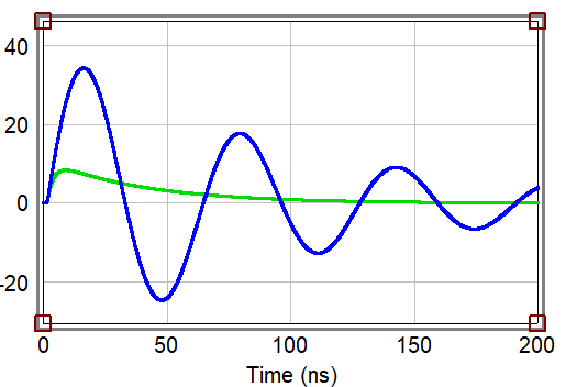
What makes the MM frightening is that the resistance is almost zero. The impedance of the discharge path is set mainly by the surge impedance √(L/C) = √(0.5 µH / 200 pF) ≈ 50 Ω, so even at a charging voltage of 200 V the peak current reaches 200 V / 50 Ω ≈ 4 A. At the same voltage, a far larger current than the HBM (R = 1.5 kΩ) flows, and it flows in nanoseconds.
Why it destroys semiconductors
The input gate of a CMOS device is a well-insulated electrode whose dielectric is an oxide film only a few to a few tens of nanometres thick. When the large ESD current passes through that film, localised Joule heating punches through the insulation at a single point.
The destructive power of the MM comes from the size of the peak current and the speed of its rise. With almost no resistance, the stored charge is released in one go. In energy terms, E = ½ × C × V²: with C = 200 pF and V = 200 V, E = ½ × 200×10⁻¹² × (200)² = 4 µJ. That looks small, but it is delivered in tens of nanoseconds and carries a peak current of several amperes — fatal for a thin dielectric.
A further problem arises in equipment where the input terminal goes to a connector. While the connector is unmated the CMOS input stays well insulated and charges easily, and the discharge happens at the instant of mating.
Choosing ESD and surge protection devices
The basic countermeasure against ESD and surge is to clamp with a protection device. Here are the main types.
TVS diode (transient voltage suppressor)
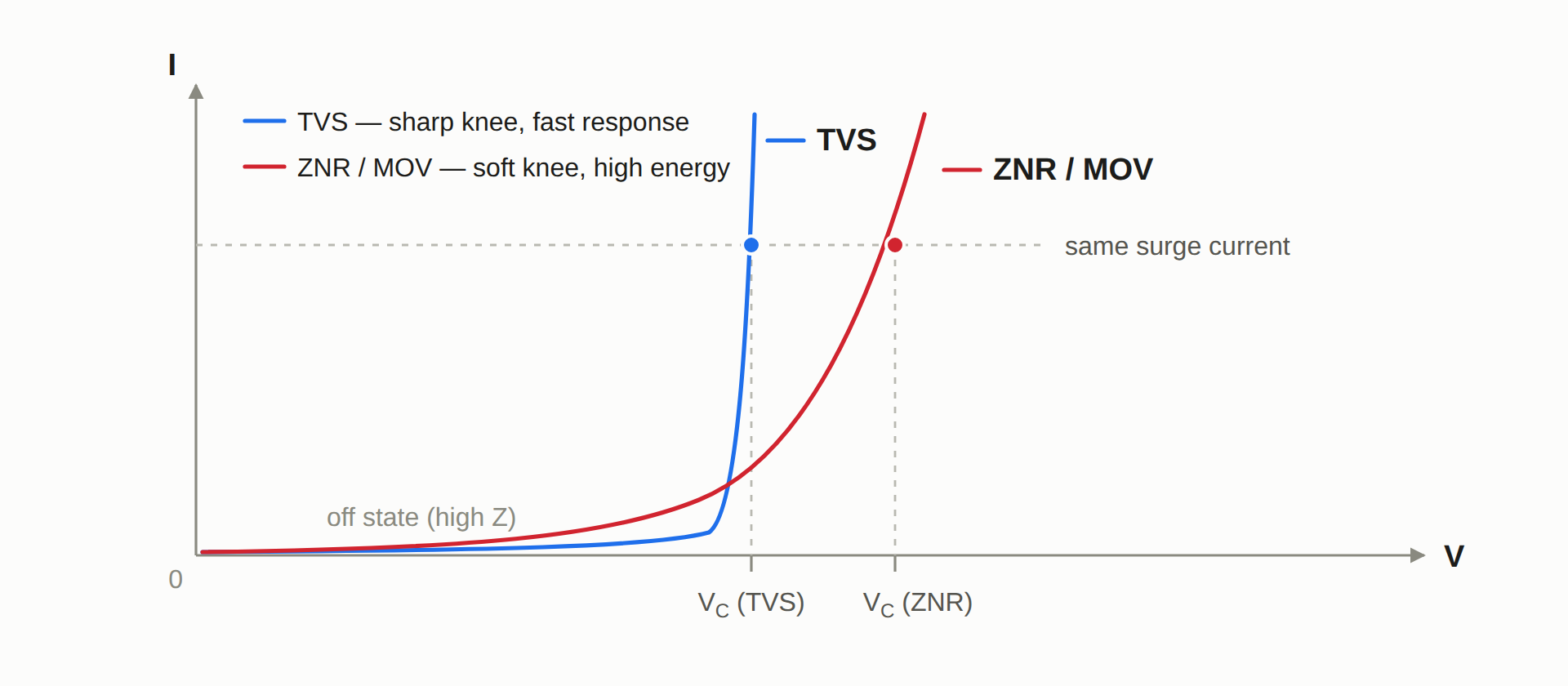
A kind of Zener diode. It is non-conducting normally, but the moment the voltage exceeds its set clamping voltage it becomes low-impedance and absorbs the excess. Its response is extremely fast — picosecond order — so it copes with sharp surges such as ESD.
- Unidirectional type: for one-way surges, much like a rectifier diode
- Bidirectional type: also handles AC and reverse surges. Widely used to protect signal lines
Varistor (ZNR / MOV)
A device whose impedance drops sharply as the voltage rises (a voltage-dependent resistor). Its characteristic is symmetrical, so it works in both directions. Its response is somewhat slower than a TVS, but it absorbs more energy, which suits it to protecting power lines.
GDT (gas discharge tube)
Absorbs the surge using an arc discharge in the enclosed gas. Its clamping voltage is relatively high (tens of volts and up) and it handles large-current surges such as lightning. Used on telephone lines, antenna systems and the like.
Placing protection devices, and how to think about it
Put the protection device as close as possible to the input terminal. The point is to clamp the surge before it gets into the board.
To get the most out of a protection device you also have to minimise the inductance of its connection path. If the trace from the device to GND is long, the L × di/dt voltage drop cancels out what the device is doing. For a discharge with a fast rise — a large di/dt, as in the MM — this trace inductance matters especially.

Staged protection is also effective. A GDT at the connector entrance for large currents plus a TVS inside the board for fast, precise clamping copes with both large and small surges.
ESD control in manufacturing
Separate from ESD protection in the finished product, ESD control during manufacturing and assembly matters too. As the machine model shows, a discharge from charged equipment or a jig produces a very large peak current. A CMOS input terminal remains well insulated until it is wired up, and even a small amount of charge destroys it.
Basic measures on the factory floor:
- Cover the workbench with a conductive mat and earth it through a high resistance (around 1 MΩ)
- Have operators wear a metal wrist strap, earthed the same way
- Use conductive flooring and conductive shoes (0.1–100 MΩ or so, since too low a resistance is an electric-shock hazard)
- Use ionisers to ionise the air so that charge dissipates naturally
- Store and transport components in conductive (ESD) bags
The reason for earthing through a high resistance is that earthing an already-charged object abruptly would let a large current flow and destroy the device. The aim is to bleed the charge away slowly.
Summary
- Static electricity is generated by friction, and both people and metal objects (equipment, jigs) become charged. It is most common in the dry winter season
- The equivalent circuit for ESD depends on the source: a person is HBM (100 pF / 1.5 kΩ, exponential decay), a metal object is MM (200 pF / 0 Ω, damped oscillation)
- Because R ≈ 0 in the MM, the path inductance resonates with C and the result is a damped oscillation. Above the critical resistance 2√(L/C) it turns into exponential decay
- With almost no resistance, the MM reaches peak currents of several amperes even at a few hundred volts — enough to destroy a thin CMOS dielectric
- Place protection devices (TVS, varistor, GDT) right at the connector, with the shortest possible path to GND
- On the production floor, conductive flooring, wrist straps and ionisers are essential

Comment