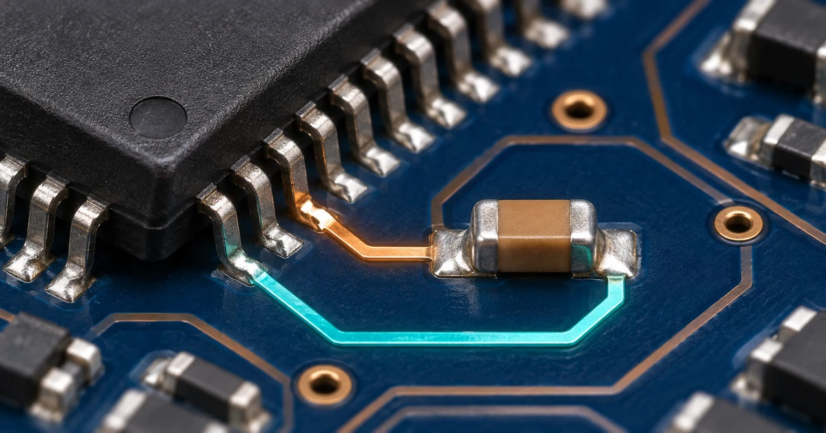
A 100 nF capacitor sits right beside the IC. One pad has a short connection to the supply pin. What happens if the trace from the opposite pad takes a detour to the ground via?
In our previous article, we treated the connection inductance as a single element. This time we split it between the supply and ground sides. With a load rising from 0 to 100 mA in 2 ns, increasing only the ground-side inductance from 0.5 to 5 nH takes the minimum voltage across the IC pins from 3.225 V to 3.065 V. Follow the current around the loop to see why.
The return path behind the ground symbol
When the IC suddenly draws current, the charged capacitor supplies it through the trace to the supply pin. The current flows through the load and leaves the ground pin. It still has to get back across the board to the other capacitor terminal.
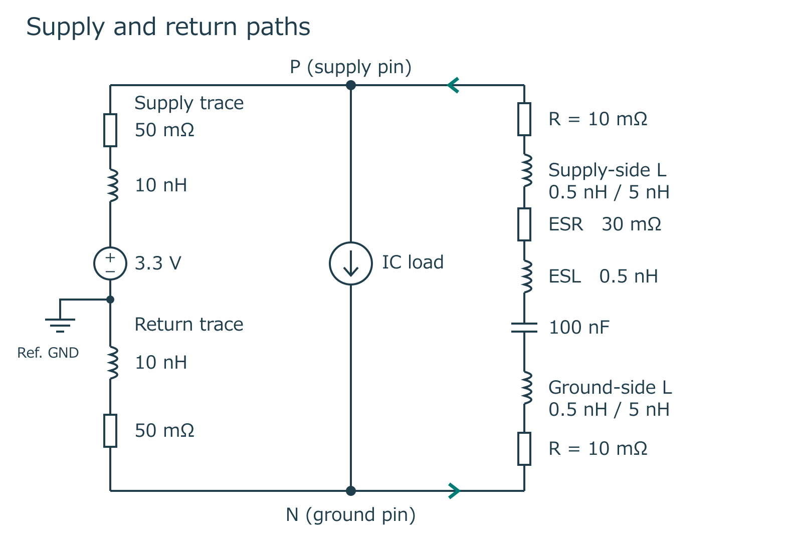
P is the IC supply pin and N is its ground pin. The negative terminal of the 3.3 V source is the voltage reference. A return trace connects N to that reference. Giving both nodes the same ground symbol would short out the very voltage we want to examine.
One capacitor, four ways to connect it
A current source models the IC load: it rises to 100 mA in 2 ns, stays there for 100 ns, then returns to zero in 2 ns. The source-side supply and return traces each have 50 mΩ and 10 nH. The capacitor has 30 mΩ equivalent series resistance (ESR) and 0.5 nH equivalent series inductance (ESL). Each capacitor connection adds 10 mΩ. Only the two connection inductances in the right branch vary.
| Case | Supply-side L | Ground-side L | Branch L incl. ESL |
|---|---|---|---|
| A | 0.5 nH | 0.5 nH | 1.5 nH |
| B | 0.5 nH | 5 nH | 6.0 nH |
| C | 5 nH | 5 nH | 10.5 nH |
| D | 5 nH | 0.5 nH | 6.0 nH |
The values 0.5 and 5 nH isolate the effect of changing one side. Their corresponding trace lengths on a real board depend on the stackup and on how closely the outgoing and return paths run together.
Measure across the IC pins
The IC sees the difference P − N. Figure 2 shows that voltage calculated from the equivalent circuit. The lower panel zooms in on the load-current rise from 200 to 202 ns.
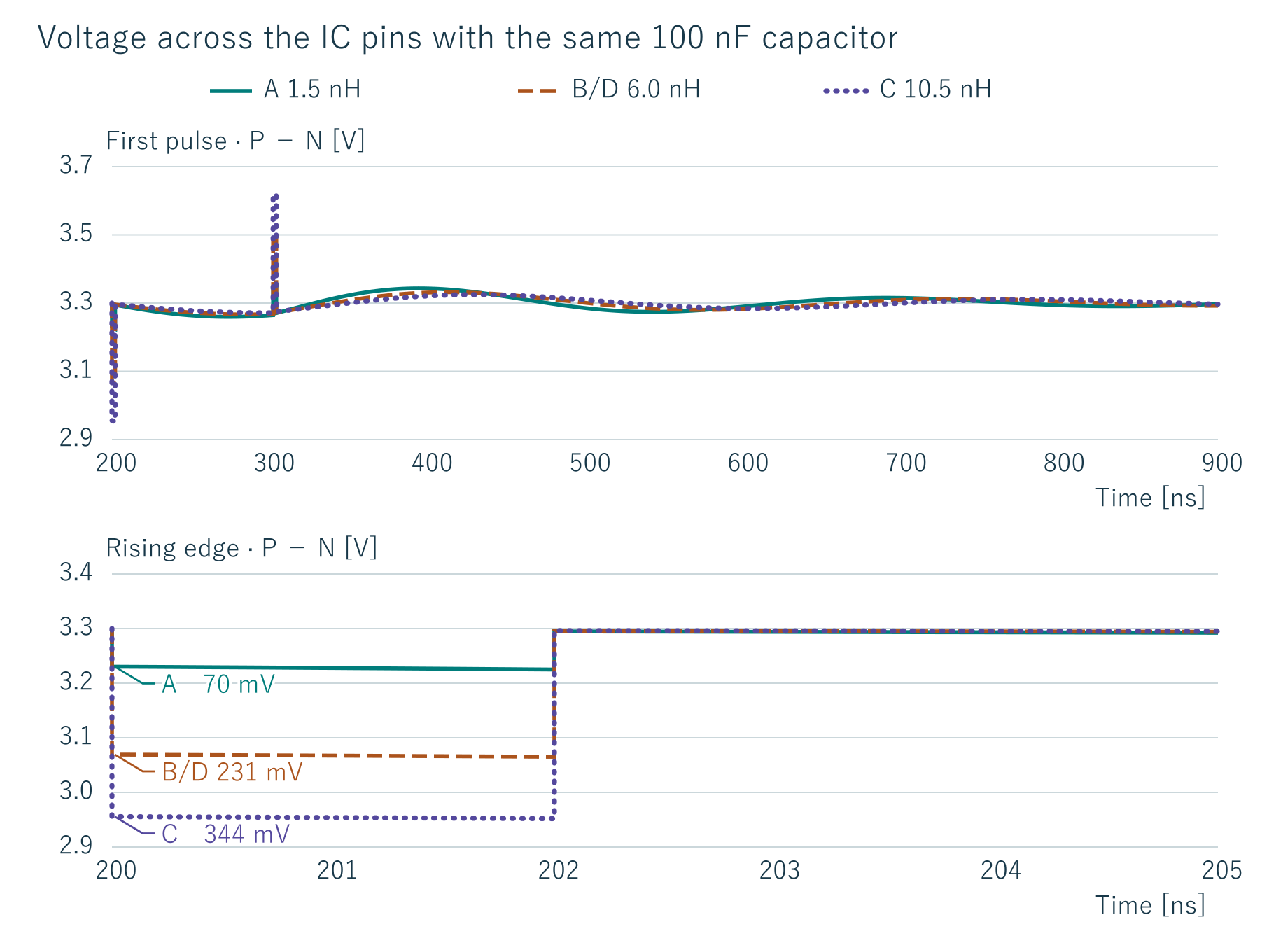
The slow oscillation after the pulse comes from the 100 nF capacitor resonating with both the 20 nH upstream loop and the capacitor branch inductance. In A their sum is 21.5 nH. Ignoring damping gives about 3.4 MHz, or 290 ns per cycle, consistent with the roughly 300 ns between peaks.
The vertical steps in the lower plot have a different origin. At 200 ns the slope of the ideal trapezoidal load current changes abruptly from zero to 0.05 A/ns. Multiply that slope by the parallel combination of the upstream and capacitor-branch inductances. For A the step is 0.05 A/ns × (20 nH ∥ 1.5 nH) ≈ 70 mV. It is about 231 mV in B and D and 344 mV in C. In B that first step accounts for most of the 235 mV dip just before 202 ns.
Halving the rise time to 1 ns at the same 100 mA doubles the slope and the initial step. The step sizes rank A < B = D < C. The minima below are for a 2 ns rise.
| Case | Minimum IC voltage [V] | IC p-p [mV] | Ground max/min [mV] | Ground p-p [mV] |
|---|---|---|---|---|
| A | 3.225 | 118.1 | +37.5 / −21.6 | 59.1 |
| B | 3.065 | 437.8 | +117.4 / −101.5 | 218.9 |
| C | 2.952 | 667.4 | +174.0 / −159.7 | 333.7 |
| D | 3.065 | 437.8 | +117.4 / −101.5 | 218.9 |
Peak-to-peak (p-p) is the maximum minus the minimum over 200–900 ns. Ground voltage is measured at N relative to the source negative terminal.
Only the ground connection changes from A to B. When the load reaches 100 mA, the capacitor contributes about 93 mA in A and 77 mA in B. In those 2 ns the upstream contribution rises by about 7.2 and 23 mA, respectively. A’s average slope of 3.6 mA/ns across 20 nH gives about 72 mV; B’s 11.6 mA/ns gives about 230 mV. By comparison, 23 mA through the 100 mΩ round-trip resistance drops only 2.3 mV. The minima differ by about 160 mV.
From C to B, reducing only the supply-side connection from 5 to 0.5 nH raises the minimum from 2.952 to 3.065 V. The 5 nH ground connection and the component ESL remain. A tenfold improvement on one side reduces the total from 10.5 to 6.0 nH, about 57% of its original value.
Swap the connections instead: B and D coincide. There is no tap in the capacitor branch, so every series element carries the same current. Seen from P and N, both cases have the same resistance, 100 nF and 6.0 nH.
Why does the IC ground pin move?
Just before the load reaches 100 mA in B, the source supplies about 23 mA and the capacitor 77 mA. P falls about 117 mV below 3.3 V while N rises about 117 mV above the reference. Together they produce a dip of about 235 mV across the pins.
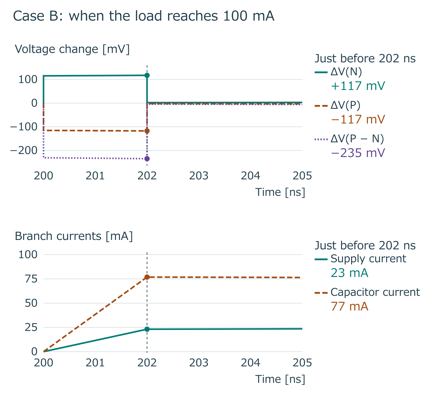
For current I returning to the source, V(N) = R_return × I + L_return × dI/dt. The 5 nH on the capacitor ground connection is in the other branch. Increasing it changes the current split, which changes the voltage developed across the upstream return. Equal resistance and inductance in the upstream outgoing and return traces give equal and opposite changes at P and N. This is why ground p-p is half the IC p-p in the table.
Start at the other pad on the board
Follow the copper from the supply pin to the capacitor. Now start at its other pad: is the ground via nearby? Does the route through the plane back to the IC ground pin stray far from the outgoing path? Measuring component spacing alone misses that detour.
On a real board current spreads in the plane and the two paths are magnetically coupled. Loop inductance depends on their separation; it is not simply the sum of isolated trace inductances. The 5 nH value belongs to an uncoupled series model, which is why swapping B and D gives the same result. P and N are board-level pins. Package inductance and on-die capacitance are omitted, so these curves do not give the on-die voltage.
Follow the loop back to the capacitor
With the capacitor still beside the IC, changing only the ground connection reduced the minimum by about 160 mV for a 2 ns edge. B and D show what matters in this series model: the sum of both connections and the capacitor ESL. When reviewing a layout, follow the path to the supply pin and then trace the return from the IC ground pin all the way back to the opposite pad.
Calculation conditions
Initially the load current is zero and the capacitor is charged to 3.3 V. The first pulse starts at 200 ns and repeats every 1 µs. Calculation and output intervals are 0.1 ns over 0–2 µs. Voltage peaks include both limits at each corner of the ideal trapezoid. Repeating A at 0.05 ns gave the same IC and ground p-p values to the precision shown.
Related reading
For the ground-pin movement in Figure 3, see Why ground bounce moves the local ground voltage. For the board return in Figure 1, see Single-point ground or ground plane? How frequency changes the choice.

Comment