This guide explains how to use the Line Calculation tool in uSimmics (formerly QucsStudio) to compute the characteristic impedance of a microstrip transmission line. It covers the physical parameters that govern impedance, how to enter substrate data, and how to solve both forward (width → impedance) and inverse (impedance → width) problems.
What You’ll Learn
- What characteristic impedance is and why it matters in PCB design
- Which physical parameters affect characteristic impedance (trace width, dielectric constant, substrate height, etc.)
- How to launch and use the Line Calculation tool in uSimmics (formerly QucsStudio)
- How to enter substrate parameters (εr, tanδ, copper thickness) correctly
- How to compute trace width for a target impedance, and how to back-calculate impedance from a known trace width
1. Characteristic Impedance
Characteristic impedance is the ratio of voltage to current in a transmission line for a traveling wave. Measured in ohms (Ω), it is an intrinsic property of the line’s geometry and materials — independent of line length.
An analogy: just as fluid flow in a pipe depends on pipe diameter and material, electrical signal flow on a PCB trace depends on the trace’s physical dimensions and the surrounding dielectric. Characteristic impedance quantifies this relationship.
2. Why Characteristic Impedance Matters
When the impedances of a signal source, transmission line, and load are all equal, signals travel with minimal reflection and loss. A mismatch causes part of the signal to reflect, leading to:
- Signal reflections: Reflected waves return to the source, degrading signal fidelity
- Data errors: Increased ringing and undershoot in high-speed digital signals
- Increased EMI: Standing waves from reflections become sources of unwanted radiation
Impedance control is especially critical for high-speed digital signals (above 1 Gbps) and RF signals (UHF and above). The standard characteristic impedance for RF systems is 50 Ω.
3. Parameters That Govern Microstrip Impedance
Trace Width (W)
Trace width is inversely proportional to characteristic impedance — wider traces give lower impedance, narrower traces give higher impedance. For 50 Ω design, there is an optimal width that depends on substrate material and thickness.
Trace Thickness (T)
The conductor (copper foil) thickness. Thicker copper reduces impedance slightly by widening the effective current path. Common values are 18 µm (0.5 oz) and 35 µm (1 oz).
Substrate Dielectric Constant (εr)
The relative permittivity of the substrate material. Higher εr slows signal propagation and lowers impedance. Representative values:
| Substrate Material | εr |
|---|---|
| FR-4 | 4.2–4.8 (typically 4.5) |
| Rogers RO4003C | 3.55 |
| PTFE (Teflon) | 2.1–2.2 |
| Alumina | 9.5–10 |
Substrate Height (H)
The thickness of the dielectric between the trace and the ground plane. A thicker substrate reduces capacitance and increases impedance.
Loss Tangent (tanδ)
The dielectric loss factor. It does not directly affect characteristic impedance but does affect transmission loss (insertion loss). Low tanδ materials are required for high-frequency applications.
Conductor Resistivity
The electrical resistivity of the conductor (copper: 1.72 × 10⁻⁸ Ω·m). The effect on characteristic impedance is negligible, but it contributes to transmission loss.
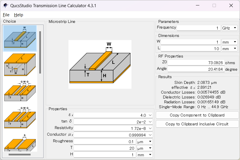
4. Computing Characteristic Impedance with uSimmics (formerly QucsStudio)
Example Calculation Conditions
| Parameter | Value |
|---|---|
| Substrate material | FR-4 |
| Dielectric constant (εr) | 4.5 |
| Substrate height (H) | 1.5 mm |
| Copper thickness (T) | 35 µm (1 oz) |
| Target impedance | 50 Ω |
Step 1: Launch Line Calculation
- From the menu bar, select Tools.
- Click Line Calculation to open the tool.
- The Line Calculation window appears.
Step 2: Select Transmission Line Type
- From the choice dropdown, select Micro Stripline.
- The parameter input fields for microstrip geometry are displayed.
Step 3: Enter Substrate Parameters
Enter the following values in the Properties section:
| Parameter | Value | Description |
|---|---|---|
| εr | 4.5 | FR-4 relative permittivity (verify with substrate datasheet) |
| tanδ | 0.02 | FR-4 loss tangent (affects high-frequency insertion loss) |
| Resistivity | 1.72 × 10⁻⁸ | Copper resistivity (Ω·m) |
| Conductor µr | 1 | Relative permeability of copper |
| Roughness | Per substrate spec | Surface roughness — becomes significant at GHz frequencies |
| T | 35 µm | Copper foil thickness |
| H | 1.5 mm | Dielectric thickness |
Enter the operating frequency in the Parameters field (e.g., 915 MHz or 2.4 GHz).
Step 4: Compute Impedance or Trace Width
Forward calculation (W → Z₀):
1. Enter the desired trace width in the W field under Dimensions.
2. Click Calculate (or the tool updates automatically).
3. The corresponding characteristic impedance Z₀ is shown.
Inverse calculation (Z₀ → W):
1. Enter the target impedance (50 Ω) in the Z₀ field.
2. The required trace width W is computed automatically.
5. Calculation Result Example
Using the conditions above (FR-4, εr = 4.5, H = 1.5 mm, T = 35 µm), achieving 50 Ω characteristic impedance requires a trace width of W = 2.77624 mm.
Use this value as the trace width specification in your PCB layout to realize the intended impedance.
Summary
Characteristic impedance is a fundamental parameter for maintaining signal integrity in PCB design. uSimmics (formerly QucsStudio)’s Line Calculation tool allows you to compute characteristic impedance instantly from trace and substrate parameters, and to back-calculate the trace width needed for a target impedance. Integrating this tool into your PCB design workflow enables accurate impedance control that minimizes signal reflections, reduces losses, and maximizes signal delivery efficiency.
Related Articles
- VSWR Analysis with uSimmics (formerly QucsStudio) [2026]
- LPF Design Guide Using uSimmics (formerly QucsStudio) [2026]
- LPF Optimization with Real Component S-Parameters in uSimmics (formerly QucsStudio) [2026]
- Stripline Characteristic Impedance Calculation in uSimmics (formerly QucsStudio) [2026]
- Monte Carlo Analysis in uSimmics (formerly QucsStudio) [2026]
Comment