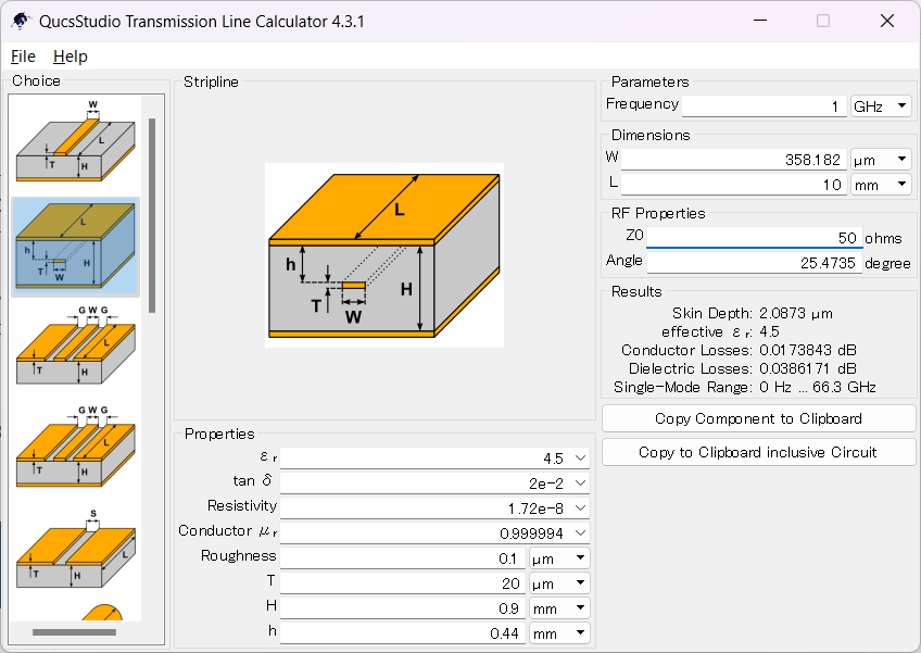
The Transmission Line Calculator in uSimmics (formerly QucsStudio) allows you to compute stripline characteristic impedance quickly and accurately. This guide covers the physical principles, substrate parameter entry, forward and inverse calculations, and practical considerations when applying results to real PCB designs.
Calculator Transmission Line Impedance Calculator Five structures: microstrip, symmetric and asymmetric stripline, and differential pairs. Handles different core and prepreg dielectric constants and trapezoidal etched conductors. →What You’ll Learn
- How stripline differs from microstrip structurally and when to choose each
- Which physical parameters determine characteristic impedance and what they mean
- Step-by-step procedure for computing stripline impedance in uSimmics (formerly QucsStudio)
- How to solve for trace width from a known impedance (inverse calculation)
- Practical considerations for applying calculated values to fabricated PCBs
1. What Is a Stripline?
A stripline is a transmission line formed by embedding a signal conductor between two parallel ground planes within a multi-layer PCB. It corresponds to routing signal traces in the inner layers of a 4-layer or higher board.
Characteristic impedance is primarily determined by three parameters:
- Signal trace width W
- Substrate relative permittivity εr
- Distance between the conductor and each ground plane (H and h)
Stripline vs. Microstrip Comparison
| Property | Stripline | Microstrip |
|---|---|---|
| Structure | Signal conductor buried between two GND planes | Surface conductor on one side, GND plane on back |
| EMI performance | Better (less radiation) | Worse (more radiation) |
| Impedance stability | High | Moderate |
| Manufacturing cost | Higher (requires multilayer board) | Lower (achievable on 2-layer board) |
| Design/rework ease | Low (buried in inner layers) | High (accessible on surface) |
Choose stripline when EMI suppression is the priority; choose microstrip when cost and design accessibility matter more.
2. Why Characteristic Impedance Control Matters
Characteristic impedance is the ratio of voltage to current for a traveling wave on a transmission line. When source, line, and load impedances are mismatched, signal reflections occur, causing:
- Ringing and overshoot at the receive end
- Increased transmission loss
- Degraded overall system performance
50 Ω is the standard characteristic impedance for RF systems.
3. Stripline Impedance Calculation in uSimmics (formerly QucsStudio)
Example PCB Specification
| Parameter | Value |
|---|---|
| Substrate material | FR-4 |
| Relative permittivity εr | 4.5 |
| Loss tangent tanδ | 0.02 |
| Conductor material | Copper |
| Conductor thickness T | 20 µm |
| Dielectric height H | 0.9 mm |
| Conductor position h | 0.44 mm |
| Target impedance | 50 Ω |
Step 1: Launch uSimmics and Open the Transmission Line Calculator
- Launch uSimmics (formerly QucsStudio).
- From the menu bar, select Tools → Line Calculation.
- From the choice dropdown, select Stripline.
Step 2: Enter Substrate Parameters
Enter the following values in the Properties section:
| Parameter | Description | Value |
|---|---|---|
| εr | Substrate permittivity. FR-4 is typically 4.5; verify with the substrate manufacturer’s datasheet | 4.5 |
| tanδ | Dielectric loss tangent. Does not directly affect impedance but impacts insertion loss at high frequencies | 0.02 |
| Resistivity | Electrical resistivity of the conductor. Copper: 1.72 × 10⁻⁸ Ω·m | 1.72e-8 |
| Conductor µr | Relative permeability of the conductor. Copper: 1 | 1 |
| Roughness | Surface roughness of the conductor. Becomes significant above a few GHz | Per substrate spec |
| T | Conductor (trace) thickness | 20 µm |
| H | Total dielectric height (distance between both GND planes) | 0.9 mm |
| h | Distance from the lower GND plane to the center of the signal trace | 0.44 mm |
Step 3: Set the Operating Frequency
In the Parameters section, enter the representative frequency for the analysis band.
Step 4: Calculate and Review
Two calculation modes are available in the Dimensions section:
Forward (W → Z₀): Enter trace width W to compute the resulting characteristic impedance Z₀.
Inverse (Z₀ → W): Enter target impedance Z₀ to compute the required trace width W.
For the substrate specification in this example, a trace width of 358 µm achieves a characteristic impedance of 50 Ω.
4. Practical Considerations
- Calculated values are theoretical; actual PCB fabrication introduces process variation.
- Etching processes create a trapezoidal trace cross-section (etching undercut) rather than the ideal rectangle, which shifts the actual impedance from the calculated value. For details, see the related article on etching undercut.
- Substrate permittivity varies with temperature, humidity, and frequency; include appropriate design margins.
- Conductor surface roughness becomes a significant contributor to insertion loss above a few GHz and should not be ignored in high-frequency designs.
5. Summary
The Transmission Line Calculator in uSimmics (formerly QucsStudio) makes stripline impedance calculation efficient and accurate. By entering precise substrate parameters and using the inverse calculation to determine required trace width, you can substantially streamline the PCB design process. Understanding the gap between theoretical calculations and actual fabrication results is essential for achieving reliable impedance management in high-frequency designs.
Related Articles
- Etching Undercut Effects on Stripline Impedance: Using uSimmics (formerly QucsStudio) [2026]
- Hybrid Substrate Characteristic Impedance Calculation in uSimmics (formerly QucsStudio) [2026]
- Footprint Pattern and Impedance Matching Optimization in uSimmics (formerly QucsStudio) [2026]
- Automatic Impedance Matching in uSimmics (formerly QucsStudio) [2026]
- Installing and Configuring uSimmics (formerly QucsStudio)
Comment