The Transmission Line Calculator in uSimmics (formerly QucsStudio) instantly computes characteristic impedance and other electrical parameters for a wide range of PCB transmission line structures. This guide uses microstrip line as an example, covering material parameter entry through to exporting the result for use in circuit simulation.
- What You’ll Learn
- What Is the Transmission Line Calculator?
- Step 1: Launching the Tool
- Step 2: Selecting a Transmission Line Type
- Step 3: Entering Material Parameters
- Step 4: Entering Dimension Parameters
- Step 5: Reading the Calculated Result
- Step 6: Importing the Result into Circuit Simulation
- Supported Transmission Line Types
- Design Tips
- Related Articles
What You’ll Learn
- How to launch the Transmission Line Calculator
- The meaning of each material and dimension parameter for microstrip line
- How to read the characteristic impedance result
- How to import the result into a uSimmics (formerly QucsStudio) circuit simulation
- The transmission line types supported and their characteristics
What Is the Transmission Line Calculator?
The Transmission Line Calculator is a built-in electrical characterization tool in uSimmics (formerly QucsStudio). It numerically computes characteristic impedance (Z₀), electrical length, effective permittivity, and propagation loss for various transmission line structures including PCB traces, coaxial cables, and waveguides.
In RF and microwave circuits, impedance mismatch on transmission lines is a primary cause of return loss and signal degradation. Accurate transmission line design is therefore directly tied to circuit performance.
Step 1: Launching the Tool
- Launch uSimmics (formerly QucsStudio).
- In the menu bar, click Tools.
- Select Line calculation from the submenu.
- The Transmission Line Calculator window opens.
Step 2: Selecting a Transmission Line Type
Use the drop-down menu at the top of the window to select the transmission line type to calculate. In this example, select Microstrip Line.
Step 3: Entering Material Parameters
For microstrip line, enter the following material parameters:
| Parameter | Example Value | Description |
|---|---|---|
| Permittivity (εr) | 4.5 | Relative permittivity of the substrate. Typical value for FR4 is around 4.5. Note frequency dependence. |
| Loss tangent (tanδ) | 0 | Dielectric loss indicator. Set to 0 to ignore loss; use the value from the material datasheet for real designs. |
| Resistivity | 0.0001 | Electrical resistivity of the conductor (copper). |
| Conductor μr | 0.999994 | Relative permeability of the conductor. Approximately 1 for copper (0.999994). |
| Roughness | 0.1 μm | Arithmetic mean roughness of the conductor surface. A typical value for electrolytic copper foil. At high frequencies, surface roughness contributes to loss via the skin effect. |
| Conductor thickness (T) | 20 μm | Copper foil thickness. Standard 1/2 oz foil is approximately 17 μm; 1 oz is approximately 35 μm. |
| Substrate height (H) | 500 μm | Thickness of the dielectric substrate (distance to the ground plane). |
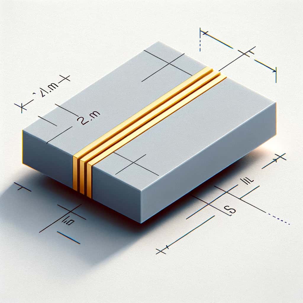
Step 4: Entering Dimension Parameters
Enter the physical dimensions of the PCB trace you want to simulate:
| Parameter | Example Value | Description |
|---|---|---|
| Width (W) | 1.0 mm | Width of the microstrip conductor strip. Wider traces result in lower characteristic impedance. |
| Length (L) | 100 mm | Physical length of the line. Used to compute electrical length. |
Step 5: Reading the Calculated Result
After parameters are entered, the Transmission Line Calculator displays results in real time.
Result for this example:
- Characteristic impedance Z₀ = 47.5176 Ω
This tells us that a 1.0 mm wide microstrip on an FR4 substrate (H = 500 μm, εr = 4.5) has a characteristic impedance slightly below 50 Ω. To achieve 50 Ω, the trace width should be reduced slightly (approximately 0.9 mm).
Step 6: Importing the Result into Circuit Simulation
- Click Copy Component to Clipboard.
- In the uSimmics (formerly QucsStudio) schematic editor, press Ctrl + V to paste the component.
- The placed transmission line component retains all calculated parameters and is ready for use in circuit simulation.
Supported Transmission Line Types
The Transmission Line Calculator handles the following transmission line structures.
Basic Transmission Lines
| Type | Characteristics |
|---|---|
| Microstrip Line | Conductor strip on one face of a dielectric substrate with a ground plane on the opposite face. The most widely used structure in high-frequency PCB design. |
| Stripline | Conductor embedded in the inner layer of a dielectric substrate. Provides strong shielding against external electromagnetic interference. Used in multilayer PCB inner layers. |
| Coplanar Waveguide | Center conductor strip flanked by ground conductors on the same surface. Low loss and suitable for high-frequency applications. |
| Coplanar Waveguide with Backside | Coplanar waveguide with an additional backside ground plane. Provides even higher shielding effectiveness. |
| Slotline | Formed by a narrow slot in a conducting plane. Has asymmetric transmission characteristics; used in balun-type elements. |
| Coaxial Cable | Dielectric material between an inner conductor and an outer shield. Wideband and stable; widely used in measurement systems and interconnect cables. |
| Twisted Pair Cable | Two copper wires twisted together. Used for differential transmission with inherent immunity to electromagnetic interference. |
| Rectangular Waveguide | Metallic tube with rectangular cross-section. Transmits only above the cutoff frequency of the dominant mode. Primarily used in microwave and millimeter-wave bands. |
Coupled Transmission Lines (for Differential Pairs and Filter Design)
| Type | Characteristics |
|---|---|
| Coupled Microstrip Line | Two electromagnetically coupled microstrip lines. Used for coupled filters and balun design. |
| Coupled Strip Line | Adjacent striplines. Used for differential routing and coupler design. |
| Coupled Coplanar Waveguide | Adjacent coplanar waveguides. Applied to devices exploiting coupling effects. |
| Coupled Coplanar Waveguide with Backside | Coupled coplanar waveguide with backside ground. Combines high shielding with controlled coupling. |
Design Tips
- The dielectric constant of FR4 varies with frequency (approximately 4.7 at low frequency, 4.2–4.5 in the GHz range). Use measured values or manufacturer data for the intended frequency band in accurate designs.
- Microstrip characteristic impedance depends strongly on the W/H ratio (trace width to substrate height). Adjusting this ratio is the primary method for targeting 50 Ω or another specific impedance.
- As of 2026, impedance calculation with this tool remains a valid starting point for differential pair routing in high-speed digital signal design.
Related Articles
- How to Use Filter Synthesis in uSimmics (formerly QucsStudio) [2026]
- How to Use Create Matching Circuit in uSimmics (formerly QucsStudio) [2026]
- How to Use Qucsattenuator in uSimmics (formerly QucsStudio) [2026]
- How to Import S-Parameter Files in uSimmics (formerly QucsStudio) [2026]
- How to Export S-Parameters in uSimmics (formerly QucsStudio) [2026]

Comment