
In high-frequency PCB design, the land patterns used to mount components introduce parasitic capacitance that alters the characteristic impedance of the transmission line. This article explains how to quantify the effect of a footprint pattern using uSimmics (formerly QucsStudio) and how to mitigate impedance degradation through a practical design countermeasure.
What You’ll Learn
- Why footprint pad geometry causes impedance discontinuities in RF circuits
- How to model and simulate the impedance impact of a U.FL connector footprint in uSimmics (formerly QucsStudio)
- The mechanism by which parasitic capacitance lowers characteristic impedance
- A concrete design countermeasure — GND plane clearance — to reduce parasitic capacitance
- How to verify the improvement effect using S-parameter simulation
1. Why Signal Integrity Matters in RF PCB Design
In RF circuits, maintaining a consistent impedance — typically 50 Ω — throughout every element of the signal path is fundamental to preserving signal quality. Even when a transmission line is precisely designed to 50 Ω, a poorly designed land pattern at a component interface introduces an impedance discontinuity that reflects signals and increases insertion loss.
2. How Footprint Pads Affect Characteristic Impedance
Parasitic Capacitance Generation
Land patterns are designed larger than the component electrode to ensure reliable soldering and mechanical attachment. This oversized pad sits directly above the GND plane and behaves as a capacitor — this is known as parasitic capacitance.
Characteristic impedance is given by:
Z₀ = √(L/C)
A larger pad increases the capacitance per unit length C, which lowers Z₀. At GHz frequencies, even a modest pad area can cause a measurable impedance drop that cannot be ignored.
Conditions That Make the Effect Worse
- Higher frequencies (GHz range) amplify the impact of any parasitic capacitance
- Having a GND plane directly beneath the pad maximizes capacitance
- Larger pad area increases capacitance proportionally
3. U.FL Connector Footprint Simulation
PCB Design Specification
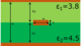
The following 4-layer PCB is used as the example. The transmission line is a microstrip on L1 (top copper), referenced to L2 (inner GND plane).
| Parameter | Value |
|---|---|
| Substrate material | FR-4 |
| Relative permittivity εr | 4.5 |
| Dielectric thickness H (L1–L2) | 100 μm |
| Conductor thickness T | 18 μm |
| Target impedance | 50 Ω |
Using the Transmission Line Calculator in uSimmics (formerly QucsStudio), the trace width that yields 50 Ω on this stackup is 171 μm.
Simulation 1: Microstrip Alone
Simulating a 171 μm-wide microstrip produces a characteristic impedance of 50 Ω, with excellent S21 (insertion loss) across the frequency range — as expected.
U.FL Connector Recommended Footprint
The recommended land pattern dimensions for the U.FL connector (Hirose, miniature RF coaxial) are:
| Pad | Recommended size |
|---|---|
| Signal pin | 1.0 mm × 1.0 mm (square) |
| GND pads | Follow connector outer footprint outline |
These dimensions are mechanically appropriate, but their RF impact needs to be verified.
Simulation 2: Effect of the Footprint Pad
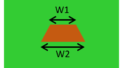
Model the footprint pad in the Transmission Line Calculator using the same substrate parameters as the microstrip, with W = 1.0 mm and L = 1.0 mm.
Simulation comparison:
- Red: Microstrip only (50 Ω)
- Blue: Microstrip + U.FL footprint pad
The results show that adding the footprint pad drops the impedance significantly below 50 Ω. The S21 degradation becomes progressively worse at higher frequencies. The root cause is the increased parasitic capacitance from the large 1.0 mm × 1.0 mm pad sitting above the L2 GND plane.
4. Countermeasure: Reducing Parasitic Capacitance
Core Strategy
Parasitic capacitance is approximated by:
C ≈ ε₀ × εr × (area A) / (distance d)
To reduce C, you can either reduce pad area or increase the distance to the GND plane. Because shrinking the signal pad below soldering minimums is often not feasible, increasing the effective distance to the GND plane is the practical option.
Concrete Solution: GND Clearance Under the Footprint
Adding a copper void (clearance) in the inner GND layer directly beneath the footprint pad increases the effective distance between the pad and ground, thereby reducing parasitic capacitance.
Implementation procedure:
- On the L2 (or L3) GND plane, create a GND clearance (void) in the area directly under the U.FL footprint.
- Size the clearance slightly larger than the pad — typically 0.2–0.5 mm of additional margin on each side.
- The increased effective gap to the GND plane reduces parasitic capacitance.
Simulation 3: Verification with GND Clearance Applied
Update the simulation model to reflect the GND clearance and re-run the S-parameter simulation.
Results with GND clearance:
- Parasitic capacitance is reduced as the effective pad-to-GND distance increases
- S21 degradation improves across the frequency range
- Characteristic impedance recovers toward 50 Ω
This simulation quantitatively confirms that GND clearance beneath the footprint is an effective countermeasure.
5. Footprint Design Guidelines for RF PCBs
| Item | Recommendation |
|---|---|
| Land size | Design to the smallest size consistent with soldering requirements; avoid unnecessary enlargement |
| GND clearance | Place a clearance void in the inner GND layer directly under RF component footprints |
| Simulation verification | Always run S-parameter simulation with the footprint included in the model |
| Frequency coverage | Simulate at the highest operating frequency to capture the worst-case impact |
| Stackup coordination | Larger dielectric thickness to the GND reference reduces parasitic capacitance; optimize together with stackup design |
6. Summary
Achieving precise characteristic impedance in RF PCB design requires attention not only to the transmission line geometry, but also to the footprint pads at component attachment points. The uSimmics (formerly QucsStudio) simulations in this article demonstrate that the U.FL connector footprint introduces parasitic capacitance that measurably lowers impedance — and that the effect grows worse at higher frequencies. Adding a GND copper void directly beneath the pad is an effective and practical countermeasure. Verifying the improvement through simulation before committing to manufacturing improves first-pass design quality and board-level RF performance.
Related Articles
- Stripline Characteristic Impedance Calculation Guide Using uSimmics (formerly QucsStudio)
- How Etching Undercut Affects Stripline Impedance — Correction Workflow in uSimmics (formerly QucsStudio)
- Characteristic Impedance Calculation for Hybrid PCBs with Mixed-Dielectric Layers Using uSimmics (formerly QucsStudio)
- Automatic Impedance Matching in uSimmics (formerly QucsStudio)
- Extracting Equivalent Circuit Parameters of Chip Capacitors with uSimmics (formerly QucsStudio)
Comment