The Transmission Line Calculator in uSimmics (formerly QucsStudio) assumes a single, uniform dielectric when computing stripline impedance. In practice, 4-layer, 8-layer, and higher-layer-count PCBs are often built from multiple substrate materials with different permittivities. This article explains how to handle that situation using the weighted-average method to derive an effective permittivity — and how to apply it in uSimmics (formerly QucsStudio).
- What You’ll Learn
- 1. The Permittivity Complexity of Multilayer PCBs
- 2. How Permittivity Determines Stripline Characteristic Impedance
- 3. Example Hybrid Board Construction
- 4. Calculating Effective Permittivity Using the Weighted-Average Method
- 5. Computing Characteristic Impedance in uSimmics (formerly QucsStudio)
- 6. Accuracy Considerations and Limitations
- 7. Summary
- Related Articles
What You’ll Learn
- Why mixed-dielectric layer stacks arise in multilayer PCB design
- Which parameters govern stripline characteristic impedance and how permittivity enters the formula
- How to calculate an effective permittivity using the weighted-average method
- How to enter the effective permittivity into uSimmics (formerly QucsStudio) and compute characteristic impedance
- Practical limitations of the approximation and when to reach for full electromagnetic simulation
1. The Permittivity Complexity of Multilayer PCBs
As PCB designs grow in density and complexity, 4-layer, 8-layer, and 16-layer boards have become standard. Mixed-dielectric stacks arise for several reasons:
- Core and prepreg materials have different permittivities (FR-4 typically ranges from 4.3 to 4.8 depending on material lot and frequency)
- A specific layer may use a low-permittivity material (such as PTFE-based laminates with εr ≈ 2.2–3.5) to achieve better high-frequency performance
- A cost-optimized hybrid stack places specialty material only on layers that carry high-frequency signals, while the remaining layers use standard FR-4
In these hybrid constructions, standard impedance formulas that assume a single εr cannot be applied directly. An appropriate approximation for the effective permittivity is required.
2. How Permittivity Determines Stripline Characteristic Impedance
Key Parameters
The characteristic impedance Z₀ of a stripline is determined by three primary parameters:
| Parameter | Symbol | Description |
|---|---|---|
| Dielectric thickness | h | Total thickness of dielectric between GND planes |
| Conductor thickness | T | Signal trace thickness |
| Conductor width | W | Signal trace width |
The IPC-based approximation formula is:
Z₀ = (60 / √εr) × ln(4h / (0.67π(0.8W + T)))
where εr is the substrate relative permittivity. This formula applies directly when the dielectric is homogeneous. With mixed layers it cannot be used without first computing an equivalent εr.
Single-Dielectric Calculation Reference
For the step-by-step single-dielectric stripline calculation workflow, see the dedicated article linked in the Related Articles section below.
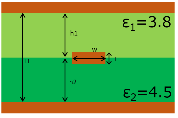
3. Example Hybrid Board Construction
The following 4-layer board is used as the worked example in this article.
| Layer | Content | Material | Relative permittivity εr | Thickness |
|---|---|---|---|---|
| L1 | Top signal layer | — | — | — |
| L1–L2 dielectric | Dielectric layer 1 | Prepreg (Material A) | εr1 = 3.8 | h1 = 400 μm |
| L2 | Inner GND plane | — | — | — |
| L2–L3 dielectric | Dielectric layer 2 | Core (FR-4) | εr2 = 4.5 | h2 = 500 μm |
| L3 | Inner GND plane | — | — | — |
| L4 | Bottom signal layer | — | — | — |
When a signal trace is routed as a stripline sandwiched between L1–L2 and L2–L3 dielectric layers, both εr1 = 3.8 and εr2 = 4.5 influence the characteristic impedance.
4. Calculating Effective Permittivity Using the Weighted-Average Method
What Is the Weighted-Average Method?
The weighted-average method computes an effective permittivity (ε_eff) for a stripline structure that spans multiple dielectric layers with different permittivities. Each layer’s contribution is weighted by its thickness.
$$\varepsilon_{\text{eff}} = \frac{\sum_{i} h_i \times \varepsilon_{r_i}}{\sum_{i} h_i}$$
Worked Example
Using the configuration above (εr1 = 3.8, h1 = 400 μm, εr2 = 4.5, h2 = 500 μm):
$$\varepsilon_{\text{eff}} = \frac{400 \times 3.8 + 500 \times 4.5}{400 + 500} = \frac{1520 + 2250}{900} = \frac{3770}{900} \approx 4.19$$
The effective permittivity is εr_eff = 4.19.
5. Computing Characteristic Impedance in uSimmics (formerly QucsStudio)
Step 1: Open the Transmission Line Calculator
- Launch uSimmics (formerly QucsStudio).
- From the menu bar, select Tools → Line Calculation to open the Transmission Line Calculator.
- Select Stripline from the choice drop-down list.
Step 2: Enter Substrate Parameters
Enter the following values in the Properties section:
| Parameter | Input value | Notes |
|---|---|---|
| εr (relative permittivity) | 4.19 (effective permittivity) | Value calculated by the weighted-average method |
| tanδ (loss tangent) | Refer to material datasheets | Weighted-average can also be applied |
| T (conductor thickness) | Actual conductor thickness | Include plating thickness |
| H (dielectric thickness) | h1 + h2 = 900 μm | Sum of all dielectric layers |
| h (conductor position) | Distance from signal trace to lower GND | Derived from the stackup drawing |
Step 3: Read the Result and Adjust Trace Width
In the Dimensions section, either enter the trace width W to read the resulting Z₀, or enter Z₀ = 50 Ω and let the tool solve for the required trace width.
Using εr_eff = 4.19 instead of either individual layer value improves agreement with measured impedance compared to using only εr1 or only εr2.
6. Accuracy Considerations and Limitations
Limits of the Weighted-Average Approximation
The weighted-average method is a reasonable practical approximation, but it has the following limitations:
- If the signal trace is positioned far from the center of the dielectric stack, approximation accuracy decreases
- When the permittivity contrast is large (for example, εr1 = 2.2 vs. εr2 = 4.5), the approximation error grows
- Non-uniform electric field distribution is not accounted for
For applications where higher accuracy is required, supplement the hand calculation with a 3D electromagnetic field simulator such as HFSS or CST.
Frequency-Dependent Permittivity
Many substrate materials, including FR-4, exhibit permittivity that varies with frequency:
| Frequency | FR-4 εr (typical) |
|---|---|
| 1 MHz | ~4.8 |
| 1 GHz | ~4.5 |
| 10 GHz | ~4.2 |
For high-frequency design, always check the substrate manufacturer’s datasheet for εr at the intended operating frequency and use that value rather than a generic figure.
7. Summary
When designing striplines on hybrid multilayer PCBs with multiple dielectric materials, the weighted-average method provides a practical way to compute an effective permittivity. Applying this value in the uSimmics (formerly QucsStudio) Transmission Line Calculator extends a single-dielectric tool to handle mixed-dielectric stacks with reasonable accuracy. For best results, use permittivity values from the substrate manufacturer’s datasheet at the target operating frequency, and include an appropriate design margin to account for manufacturing variation.
Related Articles
- Stripline Characteristic Impedance Calculation Guide Using uSimmics (formerly QucsStudio)
- How Etching Undercut Affects Stripline Impedance — Correction Workflow in uSimmics (formerly QucsStudio)
- Optimizing Footprint Patterns for Impedance Continuity in RF PCB Design with uSimmics (formerly QucsStudio)
- Automatic Impedance Matching in uSimmics (formerly QucsStudio)
- Installing and Configuring uSimmics (formerly QucsStudio)

Comment