
When we talk about noise countermeasures, we often end up with “just add a decoupling capacitor” or “just add a ferrite bead.” These can work, but if we rely only on guesswork, we may not understand why it worked, and we cannot reproduce the same result next time.
In this article, I introduce a basic framework to organize noise countermeasures. Also, using uSimmics (QucsStudio), I build a small circuit model and explain—based on the simulation waveforms—how “invisible” elements (parasitics) can change the waveform.
- Noise problems are easier if you group them into 3 types
- Basic framework: Source → Path → Victim
- Where to act first? (simple priority)
- The “invisible” culprits: parasitics (L/C/R)
- uSimmics explanation: ground is not an ideal 0 V
- Clarify the meaning of common fixes (decoupling, ferrite, ground plane)
- Summary
Noise problems are easier if you group them into 3 types
If you feel “this might be noise,” it helps to first sort the symptoms into three types.
- Malfunction: digital H/L decisions become wrong, unexpected reset, communication dropouts, false interrupts
- Performance degradation: lower receive sensitivity, worse SNR, more jitter, distorted image/audio
- Impact to others / compliance failure: failing EMI/EMC limits (radiated/conducted), interference to nearby equipment
This 3-type grouping is about symptoms. But the cause structure is similar in all cases, and it can be explained with Source → Path → Victim (example: for radiated EMI, “Source = switching,” “Path = traces/enclosure,” “Victim = nearby devices”). So we can analyze both internal issues (malfunction/performance) and external issues (EMI/EMC compliance) with the same mindset.
Basic framework: Source → Path → Victim
Noise is not a problem just because it exists. It becomes a problem only when it is generated, then couples, and then enters a sensitive point.
- Source: switching, clocks, DC/DC converters, fast I/O edges, motors/relays, etc.
- Path / Coupling: traces, power, ground, cables, space (capacitive/inductive coupling, reflection, common impedance)
- Victim: RF/receiver circuits, reference voltages, ADC, clock inputs, reset lines, sensor lines, etc.
With these three points, it becomes clearer where to apply a countermeasure.
Where to act first? (simple priority)
To reduce rework, this order is a good default.
- If you can weaken the source, that’s the strongest: slow the edge, reduce drive strength, shift frequency, use spread spectrum, etc. (trade-off with performance)
- If you cannot stop the source, control the path: ensure a good return path, reduce loop area, add termination, filtering, shielding, etc.
- Finally, make the victim more robust: so even if noise enters, it does not cause wrong decisions—add margin, stabilize the input (hysteresis/RC), and if needed, add protection parts and improve routing so it becomes “harder to enter / harder to break.”
In real hardware, “path control” is often the most effective. On PCBs, the path is strongly affected by parasitics that are not drawn in the schematic.
The “invisible” culprits: parasitics (L/C/R)
In noise problems, what matters most is often not in the schematic. The following three appear very often.
Traces and vias behave like inductors (L)
Traces, vias, and ground return paths have inductance. When current changes quickly (large di/dt), the inductance creates a voltage drop of L × di/dt.
Ideally, ground is 0 V everywhere. But real ground is connected by conductors (traces/vias), so this voltage drop makes the ground potential at that location move up and down. This is what people call ground bounce.
If ground moves, reset pins and reference voltages look like they move “relative to ground,” which can cause false reset and wrong decisions.
Adjacent traces couple like a capacitor (C)
Two nearby traces have a small coupling capacitance. Even if it is not drawn, the two traces behave as if a tiny capacitor exists between them.
When the voltage on one trace changes quickly (large dv/dt), a short current pulse flows through this coupling capacitance. That current creates a small voltage change on the other trace, and on the waveform it looks like a spike.
This “a change on one line enters another line” is crosstalk. Faster edges make larger spikes, and a higher-impedance victim line tends to show it more.
Loss (R) is also important
Ideal L and C only store and return energy. Because energy does not turn into heat, once ringing starts, it can continue for a long time.
To stop ringing, we need a way to remove energy. This is where loss (R) helps. R consumes energy as heat, so it can damp the oscillation.
This also explains why ferrite beads can work. Ferrite tends to have more loss at higher frequency, so it helps “burn off” high-frequency ringing and spikes.
uSimmics explanation: ground is not an ideal 0 V
Here we build a very small model in uSimmics and confirm by waveform that “with parasitic L, ground can move.” The goal is to understand where the path is created.
Circuit image
- VPulse (0 → 1 V pulse)
- Rload (load resistor)
- GND
- Add a small L in the ground return (example: 5 nH) to represent parasitic inductance of wiring
VPulse → Rload → node(out) → Lgnd(5nH) → GND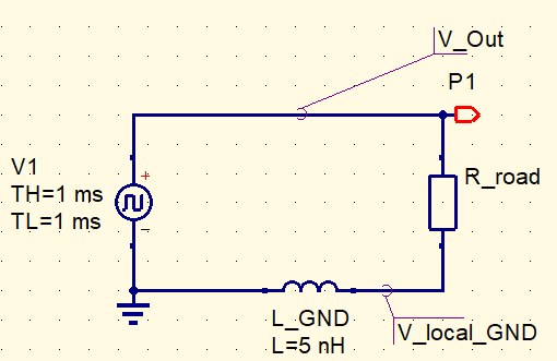
Observation points (voltage probes)
- V(out): output side of Rload (signal node)
- V(gnd_local): node on the top side of Lgnd (ground node on the circuit side)
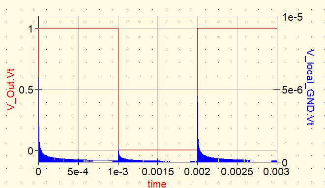
If you make the VPulse rise time faster (example: TR = 1 ns), you will see a small pulse on V(gnd_local). This is the “ground rises due to inductance in the return path” effect.
So, the problem is not only “the signal waveform is dirty.” Sometimes the reference (ground) is moving, and that can cause malfunction and performance degradation.
Clarify the meaning of common fixes (decoupling, ferrite, ground plane)
Here, we summarize what each common countermeasure is “trying to do.”
- Add a decoupling capacitor: it removes high-frequency noise near the IC so the IC supply voltage does not wobble. The key is to place it very close to the IC power pin. If it is far away, parasitic inductance of the traces blocks high-frequency current, so the effect becomes smaller.
- Add a ferrite bead: it makes high-frequency components harder to pass, so noise does not spread. For example, if DC/DC switching noise leaks into other blocks (like an RF section), place the bead at the boundary between the “noisy side” and the “clean side.” Different beads work best at different frequency ranges, so choose a part that matches your target.
- Use a solid ground plane: it provides a close return path so current does not take a long detour. A closer return path reduces loop area (go + return), which reduces radiation and unwanted coupling. But if ground is split or a signal crosses a slot, the return path may detour and become worse—so it is important to think about where the current flows.
Summary
To handle noise, first organize it with Source → Path → Victim. On PCBs, parasitics (L/C/R) that are not drawn in the schematic often create the path, and then noise enters a victim point and becomes a visible problem.
With uSimmics, a small model and waveforms can help you “feel” why a countermeasure works. In the next articles, using the same framework, we will cover reflection and ringing (termination / transmission lines), ferrite beads (why loss works), crosstalk (coupling C/L), and decoupling + ground (common impedance), step by step.
Next is signal reflection. We’ll organize why a waveform gets distorted (i.e., why it can look like “noise” suddenly appeared) using a minimal circuit.
▶ Next: What is “Reflection” in High-Speed Signals? Understand It with a Minimal Circuit


Comment