In the world of PCB design, proper management of characteristic impedance is crucial for the quality of signal transmission. This article explains the basics of characteristic impedance, its importance, and how to calculate it using QucsStudio.
1. The Concept of Characteristic Impedance
Characteristic impedance refers to the “ratio of voltage to current” in electrical signal transmission on a PCB. This ratio, a quantified index showing the relationship between voltage and current, directly affects the quality and efficiency of signal transmission. It is a measure of resistance that indicates how smoothly signals can be transmitted.
Just as the ease of water flow changes with the characteristics of a pipe, the flow of electrical signals is altered by the characteristics of the PCB. Characteristic impedance is this ease of flow expressed as a ratio of voltage to current.
When the characteristic impedance is matched, signals are transmitted smoothly, with minimal reflection and loss. However, mismatches can lead to improper signal transmission, reflections, and losses. Therefore, proper management of impedance is crucial in PCB design.
2. The Importance of Characteristic Impedance
Matching characteristic impedance is vital in PCB design to maintain signal quality and maximize the performance of electronic devices. Mismatches in characteristic impedance can lead to signal reflection and loss, adversely affecting signal quality. In the case of high-speed digital signals or high-frequency signals, these mismatches are more likely to cause data transfer errors and performance degradation. Therefore, it is crucial to accurately calculate and manage elements affecting characteristic impedance, such as PCB trace width, material, and substrate dielectric constant. Managing characteristic impedance minimizes signal reflection and loss, enhancing signal transmission efficiency.
3. Factors for Calculating Characteristic Impedance
Accurate calculation of characteristic impedance requires consideration of the following physical properties:
- Trace Width: Trace width directly relates to the resistance in the signal transmission path and is a critical factor in determining characteristic impedance. Wider traces result in lower impedance, while narrower traces have higher impedance.
- Trace Thickness: The thickness of the trace also affects impedance. Thicker traces provide a wider path for current flow, reducing impedance.
- Substrate Dielectric Constant: The dielectric constant of the substrate material affects the speed of electromagnetic wave propagation, which in turn impacts impedance. Materials with a higher dielectric constant reduce propagation speed and tend to lower impedance.
- Substrate Thickness: Especially in high-density wiring with fine trace widths, the thickness of the substrate affects capacitance and is crucial for impedance calculation.
- Separation between Trace and Substrate: Wider separation between the trace and substrate reduces capacitance, increasing impedance.
By properly setting these parameters and considering characteristic impedance, signal reflection and loss can be minimized, optimizing signal quality. Using QucsStudio to concretely calculate the effects of these elements allows for optimal PCB design.
4. Calculating Characteristic Impedance with QucsStudio
QucsStudio is a powerful tool that can calculate characteristic impedance based on these physical properties. We introduce a method to calculate the necessary trace width and substrate parameters to achieve the desired characteristic impedance using QucsStudio.
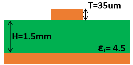
As an example, let’s calculate the characteristic impedance for a μ stripline composed of a PCB with the following specifications.
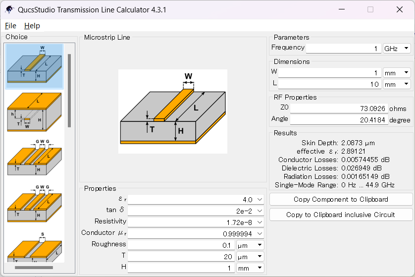
1. Launching Line Calculation
- Launch: Select Line Calculation from the ‘Tools’ menu in the QucsStudio menu bar.
- Selection of Type: Choose the structure for which you want to calculate Micro Stripline impedance from ‘choice’.
- Entering Required Parameters: Enter the parameters necessary for impedance calculation here.
2. Entering Substrate Information
First, input the substrate information in Properties.
- εr: The relative dielectric constant of the substrate. Common FR-4 is about 4.5, but it varies with the material used, so refer to the material specifications for specific values.
- tanδ: Enter the dielectric loss tangent, an indicator of electrical loss in the substrate. Adjust the number according to the material used. While it doesn’t affect characteristic impedance, it impacts transmission loss, making it important for PCBs handling high-frequency signals.
- Resistivity: Enter the resistivity of the conductor. For copper, it is 1.72×10⁻⁸Ω. This also impacts transmission loss but not characteristic impedance.
- Conductor μr: The relative dielectric constant of the conductor, not the substrate. Enter the value for the conductor being used.
- Roughness: The surface roughness of the conductor. Generally, for high-frequency applications, materials with a smoother surface are used due to the significant impact of the skin effect. Enter a value that matches the specifications of the substrate. For frequencies in the GHz order, this is not as critical.
- T: The thickness of the conductor. In this example, the substrate is 35um.
- H: The thickness of the dielectric. In this case, 1.5mm.
Next, entering the target frequency in the ‘Parameters’ in the upper right corner completes the preparation.
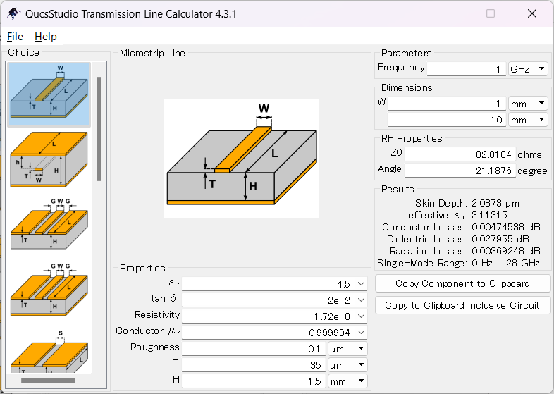
3. Verifying Characteristic Impedance
By inputting the trace width W value in ‘Dimensions’, the corresponding characteristic impedance is calculated and displayed. Conversely, by inputting a value in characteristic impedance Zo, it calculates and outputs the required trace width.
For this PCB, setting the trace width to 2.77624mm results in the formation of a microstripline with a characteristic impedance of 50Ω.
5. Conclusion
Characteristic impedance is a critical element in PCB design to maintain signal quality and maximize the performance of electronic devices. It refers to the ratio of voltage to current in the signal transmission path, indicating how smoothly signals can be transmitted.
To calculate characteristic impedance, multiple physical properties such as trace width, substrate dielectric constant, and the separation between trace and substrate GND must be considered. QucsStudio is a powerful tool for accurately calculating characteristic impedance based on these elements, enabling optimal PCB design.

コメント