In the world of high-frequency circuit design, maintaining signal transmission integrity is paramount. If the characteristic impedance of the transmission line does not match the impedance of components or connectors, it can lead to signal reflection or loss, thereby degrading the overall system performance. Even with careful adjustment of the transmission line impedance, unexpected impedance changes can occur at the point of component connection.
This article explains measures and simulation methods to avoid such issues. Specifically, it focuses on the impact of component foot patterns on impedance and introduces appropriate design and simulation techniques to maintain signal quality.
The Role of Characteristic Impedance
The characteristic impedance in the transmission line, which indicates the relationship between voltage and current, is essential for accurate signal transmission.
However, the shape of the component foot pattern can cause unexpected signal degradation. Normally, foot patterns are designed to be larger to facilitate soldering and ensure components are securely fixed, but this design can introduce unintended parasitic capacitance, negatively impacting the impedance.
In high-frequency circuit design, even these minor effects can lead to significant problems, making it crucial to understand these impacts through simulation and analysis.
U.FL Connector Foot Pattern Simulation
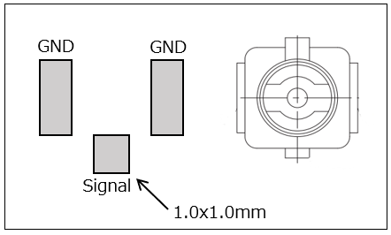
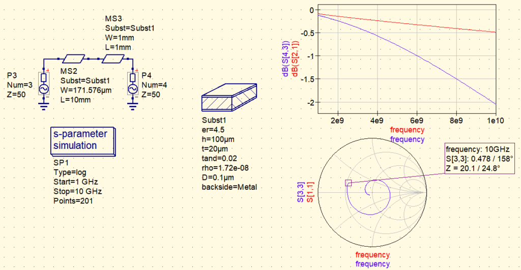
We will simulate a design example using the recommended foot pattern of the U.FL connector, a widely used coaxial connector, on a 50Ω microstrip line with Qucs Studio.
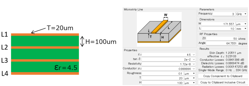
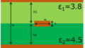
This time, we design a 50Ω microstrip line using L1 and L2 layers of the specified PCB. When designed with the “Transmission Line Calculator,” the trace width for 50Ω is 171μm.
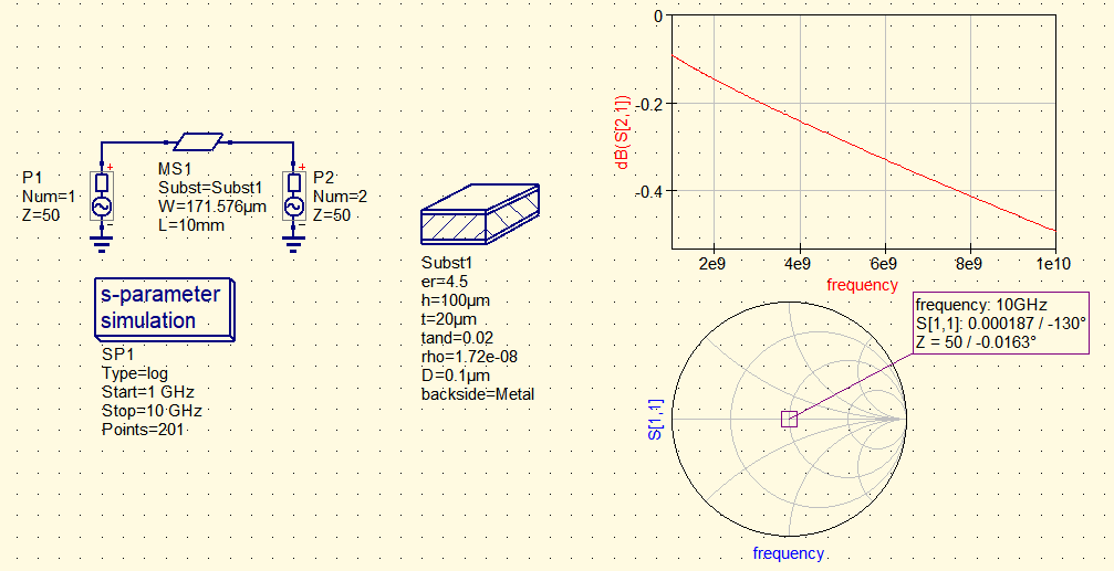
When simulating this microstrip line, we can confirm that the characteristic impedance is 50Ω, and the transmission characteristics are good.
Next, we simulate the scenario where the U.FL connector is connected to the microstrip line and observe the impact of the foot pattern.
The recommended foot pattern for U.FL suggests that the signal pin should form a land with a 1.0×1.0mm square, considering the implementation aspect.

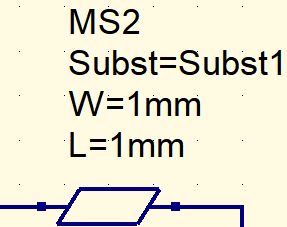
The simulation model for this land is created similarly to the microstrip line using the “Transmission Line Calculator.” The dielectric constant and height (H) of the substrate remain the same, specifying W=1.0mm and L=1.0mm.
The simulation results demonstrate that the recommended foot pattern for components can affect the characteristic impedance and potentially degrade the circuit’s transmission characteristics.
Red: Strip line only Blue: Strip line + Foot pattern
Causes of Impedance Reduction
When attaching the U.FL connector, the increase in size of the foot pattern leads to an increase in parasitic capacitance, which is a primary factor affecting the characteristic impedance.
The characteristic impedance is calculated based on the values of inductance and capacitance, and as the size of the foot pattern increases, so does the capacitance, which in turn reduces the impedance.
Solutions to Reduce Impedance Drop
To mitigate impedance reduction, optimizing the foot pattern is effective. Parasitic capacitance is determined by the size of the foot pattern and the distance to the GND layer.
Increasing the distance to the GND layer can reduce parasitic capacitance.
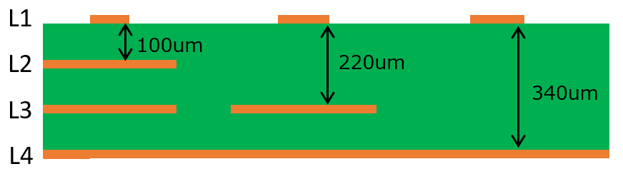
Therefore, removing the layers below the foot pattern can improve this situation.
By removing L2 or L3 layers and placing the foot pattern, you can increase the clearance to GND, thereby reducing parasitic capacitance.
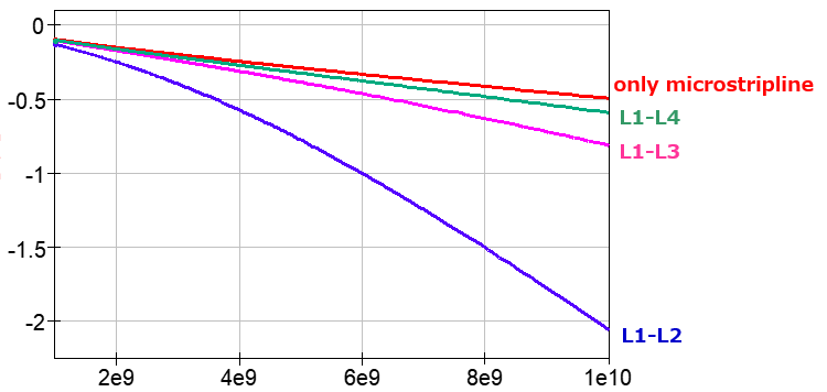
Simulating the passage characteristics of the foot pattern with increased clearance shows that expanding the distance to GND and reducing parasitic capacitance can mitigate the impact of impedance reduction.
Conclusion
This article discussed the importance of signal transmission integrity in high-frequency circuit design and the problems caused by impedance mismatch. We specifically examined the impact of component foot patterns on impedance using the U.FL connector as an example, revealing its effects through simulation.
We also touched on the importance of foot pattern optimization as a solution to impedance reduction. With this information, more effective high-frequency circuit designs can be achieved.
コメント